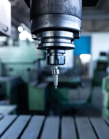
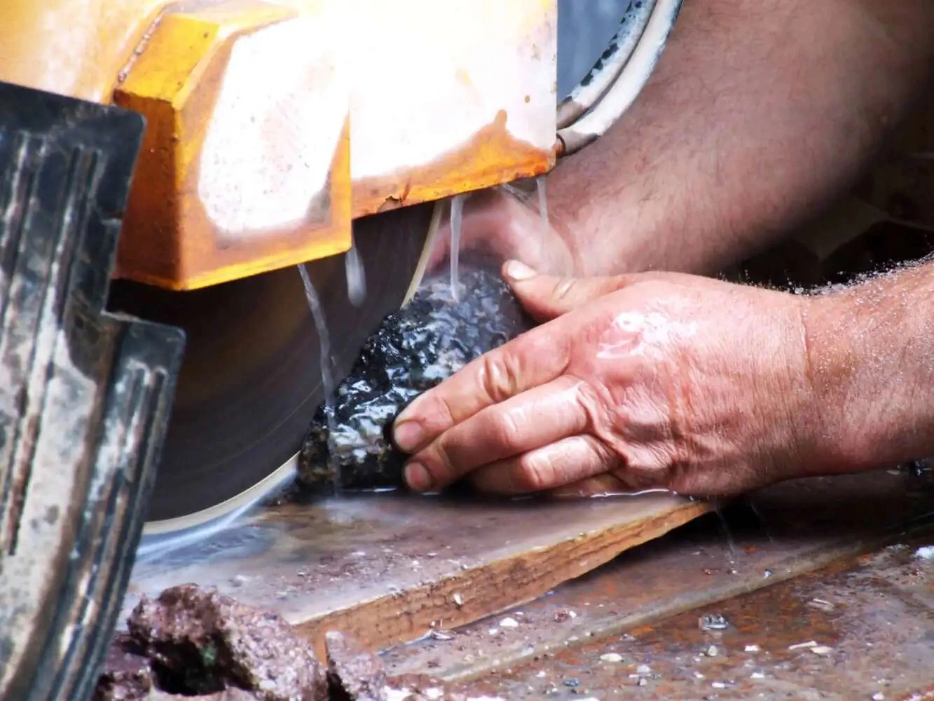
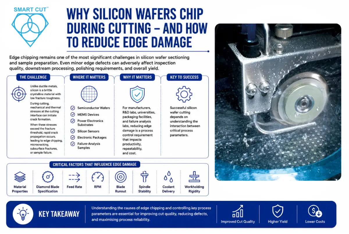
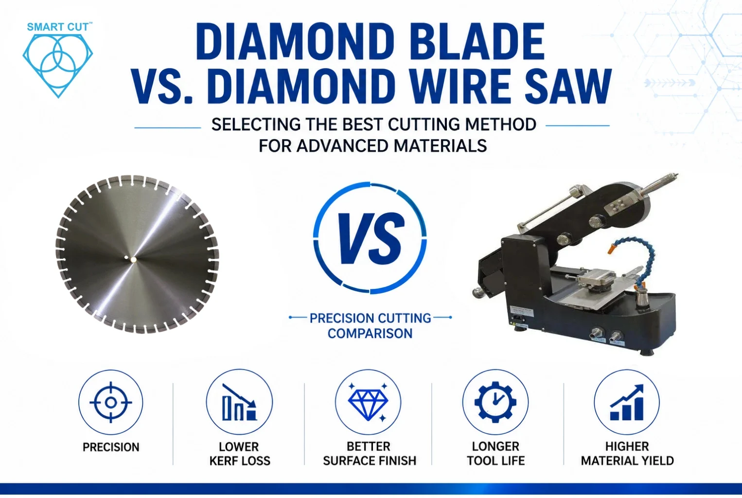
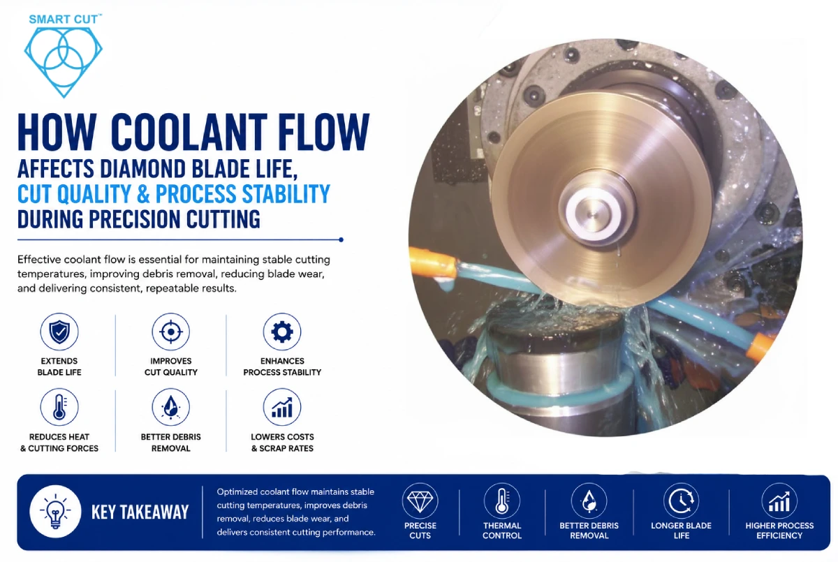
Why Silicon Wafers Chip During Cutting – And How to Reduce Edge Damage
Table of Contents
ToggleEdge chipping remains one of the most significant challenges in silicon wafer sectioning and sample preparation. Whether cutting semiconductor wafers, MEMS devices, power electronics substrates, silicon sensors, electronic packages, or failure-analysis samples, even minor edge defects can adversely affect inspection quality, downstream processing, polishing requirements, and overall yield.
Unlike ductile metals that can absorb deformation energy through plastic flow, silicon behaves as a brittle crystalline material with relatively low fracture toughness. During cutting operations, mechanical and thermal stresses generated at the cutting interface can initiate crack formation. Once these stresses exceed the material’s fracture threshold, crack propagation may occur rapidly, resulting in edge chipping, microcracking, subsurface fractures, or complete sample failure.
For semiconductor manufacturers, R&D laboratories, universities, electronic packaging facilities, and failure analysis laboratories, reducing edge damage is not simply a quality objective; it is a process control requirement that directly impacts productivity, repeatability, and cost.
Successful silicon wafer cutting depends on understanding the interaction between:
Material properties
Diamond blade specification
Feed rate
RPM
Blade runout
Spindle stability
Coolant delivery
Workholding rigidity
This article examines the engineering mechanisms underlying silicon wafer chipping and provides practical guidance for reducing damage, improving cut quality, and maximising process reliability.
Trusted by Tens of Thousands of Manufacturers, Laboratories Research Institutions Worldwide Since 1990
Established in 1990
Why This Topic Matters to Semiconductor Manufacturers
Edge chipping is not simply a cosmetic defect.
For semiconductor manufacturers, research laboratories, and electronic packaging facilities, cutting-induced damage can directly affect:
Device yield
Failure analysis accuracy
Polishing time
Sample repeatability
Inspection quality
Manufacturing costs
In many cases, the cost associated with a damaged wafer significantly exceeds the cost of the cutting operation itself.
As device geometries become smaller and material values increase, minimizing cutting-induced damage becomes increasingly important.
Why Edge Chipping Matters
Many manufacturers initially evaluate cutting quality based on dimensional accuracy.
However, edge quality is often equally important.
A wafer can meet dimensional specifications while still containing defects that compromise performance, reliability, and inspection accuracy.
Edge chipping can create:
Stress concentration points
Crack initiation sites
Reduced mechanical strength
Increased polishing requirements
Inspection challenges
Reduced device yield
Increased scrap rates
Process variability
For semiconductor manufacturers, even microscopic defects may propagate during later processing steps.
Processes such as:
Backgrinding
Polishing
Dicing
Packaging
Thermal cycling
Reliability testing
can enlarge pre-existing cracks introduced during sectioning.
As a result, a cutting defect that initially appears insignificant may later become a catastrophic failure mechanism.
The Hidden Cost of Silicon Wafer Damage
The visible chip at the edge of a wafer is often only part of the problem.
In many cases, the most significant damage occurs beneath the surface.
This hidden damage may include:
Subsurface fractures
Microcracks
Residual stress zones
Crystal lattice damage
Fracture networks
These defects frequently remain undetected until polishing or microscopy evaluation begins.
When subsurface damage is extensive, manufacturers often experience:
Increased polishing time
Lower throughput
Reduced sample reliability
Additional labor costs
Greater consumable usage
In high-value semiconductor applications, the cost of a failed sample often exceeds the cost of the cutting operation itself.
Understanding Silicon as an Engineering Material
To understand why silicon chips during cutting, it is important to understand how silicon behaves under mechanical loading.
Silicon is fundamentally different from most metals.
Rather than deforming plastically when stressed, silicon tends to fracture.
This characteristic is directly related to its crystal structure and mechanical properties.
Silicon Material Properties Relevant to Precision Cutting
| Property | Typical Value |
|---|---|
| Density | 2.33 g/cm³ |
| Crystal Structure | Diamond Cubic |
| Hardness | ~1150 HV |
| Elastic Modulus | 130–185 GPa |
| Fracture Toughness | 0.8–1.0 MPa√m |
| Thermal Conductivity | ~148 W/mK |
| Coefficient of Thermal Expansion | ~2.6 × 10⁻⁶ /°C |
| Ductility | Extremely Low |
| Brittleness | High |
These properties make silicon ideal for semiconductor applications, but also create significant machining challenges.
Because silicon possesses relatively low fracture toughness, even modest increases in cutting force can initiate crack formation.
Why Silicon Behaves Differently Than Metals
Many cutting problems occur because operators apply metal-cutting logic to brittle materials.
Metals typically absorb energy through plastic deformation.
Silicon does not.
Instead, silicon stores elastic energy until a critical stress threshold is reached.
Once that threshold is exceeded, fracture occurs rapidly with little warning.
This difference explains why relatively small changes in feed rate, blade specification, or machine stability can dramatically influence wafer quality.
Understanding Silicon Fracture Mechanics
Most edge chipping originates from fracture mechanics rather than simple abrasion.
During cutting, diamond particles penetrate the silicon surface.
Each diamond particle acts as a localized stress concentrator.
The material experiences:
Compressive stresses
Tensile stresses
Shear stresses
Thermal stresses
While compressive forces generally help stabilize brittle materials, tensile stresses are particularly dangerous.
Silicon is significantly weaker in tension than in compression.
When localized tensile stress exceeds the material’s fracture toughness, cracks begin to form.
Once initiated, cracks may:
Stop naturally
Continue propagating
Connect with other cracks
Extend beneath the surface
The final result depends on cutting conditions and process stability.
Common Causes of Silicon Wafer Chipping
| Cause | Severity | Frequency | Recommended Action |
|---|---|---|---|
| Excessive Feed Rate | High | Very Common | Reduce feed rate |
| Incorrect Blade Specification | High | Common | Optimize blade selection |
| Poor Coolant Delivery | Medium | Common | Improve nozzle placement |
| Blade Runout | High | Common | Verify spindle accuracy |
| Poor Workholding | Medium | Common | Improve fixturing |
| Excessive Vibration | High | Less Common | Improve machine rigidity |
Types of Damage Commonly Observed During Silicon Wafer Cutting
Not all damage appears the same.
Different process variables often produce different damage mechanisms.
Understanding these failure modes helps identify root causes more effectively.
Edge Chipping
Edge chipping is the most visible defect encountered during wafer sectioning.
Typical characteristics include:
Localized material breakout
Jagged wafer edges
Corner fractures
Surface discontinuities
Common causes include:
Excessive feed rates
Blade vibration
Coarse diamond grit
Poor workpiece support
Microcracking
Microcracks are small fractures that extend below the visible surface.
These defects may not be visible without microscopy.
Microcracking often leads to:
Reduced wafer strength
Reliability concerns
Unexpected failures during processing
Because these cracks are hidden, they often represent one of the most serious quality risks.
Subsurface Damage
Subsurface damage occurs beneath the cut surface.
This may include:
Fracture networks
Residual stresses
Crystal damage
Microcracking
Subsurface damage frequently determines:
Polishing time
Inspection quality
Sample usability
Many manufacturers focus only on visible edge quality while overlooking subsurface damage that ultimately drives process costs.
Breakout Fractures
Breakout fractures typically occur near the end of a cut.
As the remaining material thickness decreases, support becomes limited.
If cutting forces remain too high, large pieces of material may separate suddenly.
Common causes include:
Excessive feed pressure
Poor support conditions
Blade instability
Improper cutting strategy
How Feed Rate Influences Edge Chipping
Feed rate is one of the most important variables affecting wafer quality.
In many applications, reducing feed rate produces immediate improvements in edge quality.
As the feed rate increases:
Cutting forces increase
Blade deflection increases
Stress intensity increases
Crack propagation becomes more likely
This occurs because each diamond particle removes more material during every revolution.
Higher material removal rates generate greater localized stress concentrations.
These stresses increase the probability of crack initiation.
Typical Symptoms of Excessive Feed Rates
Manufacturers often observe:
- Increased edge chipping
- Larger breakout defects
- More microcracking
- Greater polishing requirements
- Reduced blade life
Aggressive feed rates may improve throughput in the short term, but often increase overall process costs due to scrap, rework, and reduced yield.
Balancing Throughput and Quality
One of the most common mistakes in wafering operations is assuming that slower is always better.
Extremely low feed rates may improve edge quality but reduce productivity unnecessarily.
The objective is not to minimize feed rate.
The objective is to identify the optimal process window where:
Edge quality is acceptable
Throughput remains practical
Blade wear is controlled
Process stability is maintained
Successful manufacturers typically establish feed-rate windows rather than relying on a single operating value.
How RPM Influences Silicon Wafer Quality
Spindle speed directly affects cutting mechanics.
RPM influences:
- Diamond engagement frequency
- Chip load
- Cutting forces
- Heat generation
- Surface finish quality
In general, increasing RPM reduces chip load per diamond particle.
This often produces:
- Smoother cutting action
- Reduced force fluctuations
- Improved surface quality
However, higher RPM is not always beneficial.
Excessive spindle speed may introduce new problems, including:
Thermal buildup
Coolant disruption
Increased blade wear
Dynamic instability
The optimal RPM depends on several variables:
Blade diameter
Blade bond type
Diamond concentration
Wafer thickness
Machine design
Coolant system effectiveness
Successful wafering operations optimize RPM together with feed rate rather than treating either parameter independently.
Feed Rate vs RPM: Why They Must Be Optimized Together
Many cutting problems occur because operators adjust only one variable.
For example:
Reducing the feed rate while maintaining excessive RPM may not eliminate damage.
Likewise:
Increasing RPM without addressing blade instability may actually increase vibration.
The most successful processes optimize:
Feed rate
RPM
Blade specification
Coolant delivery
as a complete system.
When these variables are balanced correctly, manufacturers often achieve:
Reduced chipping
Improved edge quality
Longer blade life
Better repeatability
Lower polishing costs
Blade Runout and Concentricity: Often Overlooked Sources of Edge Damage
Many wafering operations focus heavily on blade selection and cutting parameters while overlooking spindle accuracy.
In reality, blade runout is one of the most common contributors to inconsistent cutting performance.
Runout occurs when the blade does not rotate perfectly around its intended centerline.
Even minor amounts of runout can create:
Cyclic cutting forces
Blade vibration
Variable chip loads
Increased cutting pressure
Uneven material removal
These conditions increase stress concentrations along the cutting path and elevate the probability of crack initiation.
Why Silicon Is Sensitive to Runout
Ductile materials can often absorb process variation without immediate failure.
Silicon cannot.
Because silicon fractures rather than deforms, even small fluctuations in cutting force can generate localized tensile stresses sufficient to initiate cracking.
Common symptoms associated with excessive runout include:
Random edge chipping
Irregular surface finish
Blade wander
Dimensional inconsistency
Reduced blade life
In many cases, manufacturers mistakenly blame blade specifications when spindle accuracy is the true root cause.
Concentricity and Cutting Stability
Concentricity refers to the alignment of:
- Blade
- Arbor
- Spindle
- Flanges
- Cutting path
Poor concentricity introduces instability into the cutting process.
When concentricity errors exist, the blade experiences periodic loading variations.
This can result in:
Increased vibration
Higher cutting forces
Poor edge quality
Greater risk of breakout fractures
For semiconductor applications, maintaining cutting stability is critical.
Even small improvements in spindle accuracy often produce measurable improvements in wafer quality.
How Coolant Influences Silicon Wafer Quality
Coolant is frequently viewed as a blade life issue.
In reality, coolant is equally important for damage reduction.
A properly designed coolant system helps:
Control temperature
Reduce friction
Remove debris
Stabilize cutting conditions
Improve surface quality
Insufficient coolant delivery may cause:
Thermal stress
Blade loading
Increased cutting forces
Accelerated blade wear
Greater edge damage
Thermal Stress and Crack Formation
Although silicon has relatively high thermal conductivity, localised heat generation still occurs at the cutting interface.
Uneven heating can create thermal gradients.
These gradients generate stresses within the wafer.
When thermal stresses combine with mechanical stresses generated by the blade, fracture risk increases significantly.
Effective coolant delivery helps minimize this problem.
Coolant Delivery Location Matters
The amount of coolant is important.
The location of coolant delivery is equally important.
Coolant should reach:
- The blade-workpiece interface
- The primary heat generation zone
- The chip evacuation area
Poor nozzle positioning often reduces coolant effectiveness even when flow rates appear sufficient.
Filtration and Process Stability
Many precision cutting
operations use recirculating coolant systems.
Without adequate filtration, abrasive particles and silicon debris may continuously re-enter the cutting zone.
This can result in:
Increased scratching
Reduced surface quality
Higher blade wear
Process instability
Proper filtration helps maintain consistency and improve overall cutting performance.
Blade Thickness and Kerf Considerations
Blade thickness directly influences cutting force.
Thicker blades:
- Remove more material
- Generate higher cutting forces
- Increase kerf loss
- Produce greater heat generation
For brittle materials such as silicon, higher cutting forces generally increase fracture risk.
Advantages of Thin-Kerf Wafering Blades
Thin-kerf diamond blades help reduce:
Material loss
Cutting force
Heat generation
Edge damage
Benefits often include:
Improved wafer yield
Better edge quality
Reduced polishing requirements
Lower consumable costs
This becomes particularly important when processing expensive semiconductor materials.
Recommended Diamond Wafering Blade Selection Matrix
| Application | Typical Material Thickness | Recommended Blade Type | Priority |
|---|---|---|---|
| Thin Silicon Wafers | <500 µm | Ultra-Thin Wafering Blade | Edge Quality |
| Standard Silicon Wafers | 500 µm–2 mm | Precision Wafering Blade | Balanced Performance |
| Failure Analysis Samples | Variable | Fine-Grit Wafering Blade | Damage Reduction |
| Electronic Packages | Variable | Precision Diamond Blade | Repeatability |
| Research Materials | Variable | Fine-Grit Wafering Blade | Surface Integrity |
Important
Blade selection should always consider:
Material condition
Machine type
Throughput objectives
Surface finish requirements
Yield targets
There is no universal blade specification suitable for every application.
Process Optimization Guidelines
Successful wafer sectioning rarely depends on a single variable.
The best results are typically achieved when multiple process parameters are optimized simultaneously.
Focus Areas
Feed Rate
Reduce cutting force while maintaining practical throughput.
RPM
Maintain stable cutting conditions and minimize chip load fluctuations.
Blade Selection
Match grit size and bond characteristics to application requirements.
Coolant Delivery
Provide adequate cooling and debris removal.
Workholding
Prevent movement during sectioning.
Machine Stability
Minimize vibration and spindle errors.
Application Example: Improving Silicon Wafer Edge Quality Through Process Optimization
Application
Cross-sectional sample preparation for semiconductor failure analysis.
Material
Monocrystalline silicon wafers.
Primary Challenges
- Edge chipping
- Increased polishing requirements
- Inconsistent sample quality
Initial Process Conditions
| Variable | Initial Condition |
|---|---|
| Feed Rate | Aggressive |
| Coolant Delivery | Inconsistent |
| Blade Specification | General Purpose |
| Runout Verification | Not Routinely Performed |
Root Cause Investigation
Engineering evaluation identified multiple contributing factors:
- Excessive cutting forces
- Inadequate coolant targeting
- Blade specification not optimized for edge quality
- Lack of routine spindle inspection
Corrective Actions
Reduced feed rate
Improved coolant delivery
Implemented finer-grit
wafering blade
Verified spindle accuracy
Improved sample fixturing
Results
Following process optimization:
- Edge quality improved substantially
- Visible chipping decreased
- Polishing requirements were reduced
- Process repeatability improved
- Sample preparation consistency increased
Engineering Lesson
The greatest improvement resulted from optimizing the complete cutting process rather than changing a single variable.
Troubleshooting Guide
| Problem | Possible Cause | Recommended Action |
|---|---|---|
| Edge Chipping | Feed rate too high | Reduce feed rate |
| Microcracking | Excessive cutting force | Optimize blade specification |
| Blade Wander | Runout or instability | Verify spindle accuracy |
| Poor Surface Finish | Coarse grit blade | Use finer grit blade |
| Thermal Damage | Poor coolant delivery | Improve coolant targeting |
| Breakout Fractures | Insufficient support | Improve fixturing |
Recommended UKAM Solutions for Silicon Wafer Cutting
The optimal blade depends on:
Wafer thickness
Material characteristics
Surface finish requirements
Throughput objectives
Equipment configuration
Common solutions include:
| Application | Recommended Product Type |
|---|---|
| Thin Silicon Wafers | Precision Diamond Wafering Blades |
| Semiconductor Failure Analysis | Fine-Grit Wafering Blades |
| Electronic Packaging | Precision Diamond Blades |
| Research Applications | Ultra-Thin Diamond Blades |
| Cross-Section Preparation | Precision Sectioning Blades |
Need help selecting the correct blade specification? UKAM’s application engineers can provide recommendations based on your material, machine, and quality requirements.
Frequently Asked Questions
Common causes include excessive feed rates, blade vibration, poor coolant delivery, spindle instability, and improper blade selection.
Generally, yes, although excessively low feed rates may reduce productivity unnecessarily.
Coolant controls heat, removes debris, and stabilises the cutting process.
Yes. Even small amounts of runout can increase vibration and cutting force variation.
In many applications, thin-kerf blades reduce cutting force and improve yield.
Subsurface damage typically results from excessive cutting forces and fracture propagation beneath the visible surface.
Edge quality affects yield, reliability, polishing requirements, and inspection accuracy.
Regular inspection intervals depend on machine usage and process requirements.
No. Excessive RPM can increase heat generation and instability.
Attempting to improve throughput without understanding how feed rate, RPM, blade selection, and coolant interact.
Engineering Quick Reference Guide
| Item | Recommendation |
|---|---|
| Material | Silicon |
| Primary Risk | Edge Chipping |
| Secondary Risk | Subsurface Damage |
| Most Important Variables | Feed Rate, RPM, Coolant, Runout |
| Preferred Tooling | Precision Diamond Wafering Blade |
| Quality Objective | Minimize Fracture Damage |
| Optimization Goal | Improve Yield & Inspection Quality |
Need Help Optimizing Silicon Wafer Cutting?
Selecting the correct diamond wafering blade, feed rate, RPM range, coolant configuration, and machine setup can significantly influence edge quality and yield.
Contact UKAM’s applications engineering team for guidance on silicon wafer sectioning, damage reduction, process optimization, and blade selection tailored to your specific application.
Conclusion
Silicon wafer chipping is fundamentally a fracture mechanics problem.
The visible chip at the wafer edge is often only the surface manifestation of deeper mechanical and thermal damage occurring within the material.
Successful wafer sectioning requires understanding the interaction between material properties, blade specification, feed rate, spindle speed, coolant delivery, machine stability, and workholding conditions.
Manufacturers who optimize these variables as a complete system frequently achieve significant improvements in:
Edge quality
Process consistency
Wafer yield
Inspection reliability
Blade performance
Overall operational efficiency
For semiconductor manufacturers, research laboratories, failure analysis facilities, and advanced materials organizations, reducing cutting-induced damage is one of the most effective ways to improve downstream process performance and maximize the value of every wafer.
Trusted by Tens of Thousands of Manufacturers, Laboratories,
Research Institutions Worldwide Since 1990
Established in 1990
RELATED ARTICLES

Brian is an experienced professional in the field of precision cutting tools, with over 27 years of experience in technical support. Over the years, he has helped engineers, manufacturers, researchers, and contractors find the right solutions for working with advanced and hard-to-cut materials. He’s passionate about bridging technical knowledge with real-world applications to improve efficiency and accuracy.
As an author, Brian Farberov writes extensively on diamond tool design, application engineering, return on investment strategies, and process optimization, combining technical depth with a strong understanding of customer needs and market dynamics.
About Brian Farberov
Brian is an experienced professional in the field of precision cutting tools, with over 27 years of experience in technical support. Over the years, he has helped engineers, manufacturers, researchers, and contractors find the right solutions for working with advanced and hard-to-cut materials. He’s passionate about bridging technical knowledge with real-world applications to improve efficiency and accuracy. As an author, Brian Farberov writes extensively on diamond tool design, application engineering, return on investment strategies, and process optimization, combining technical depth with a strong understanding of customer needs and market dynamics.
View all posts by Brian Farberov

