


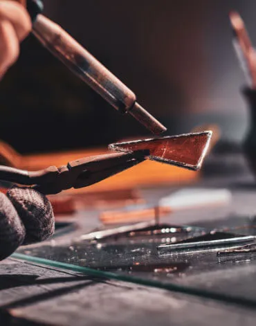


Semiconductor Wafer Grinding: 60% Reduction in Edge Chipping Using Resin Bond Diamond Wheels
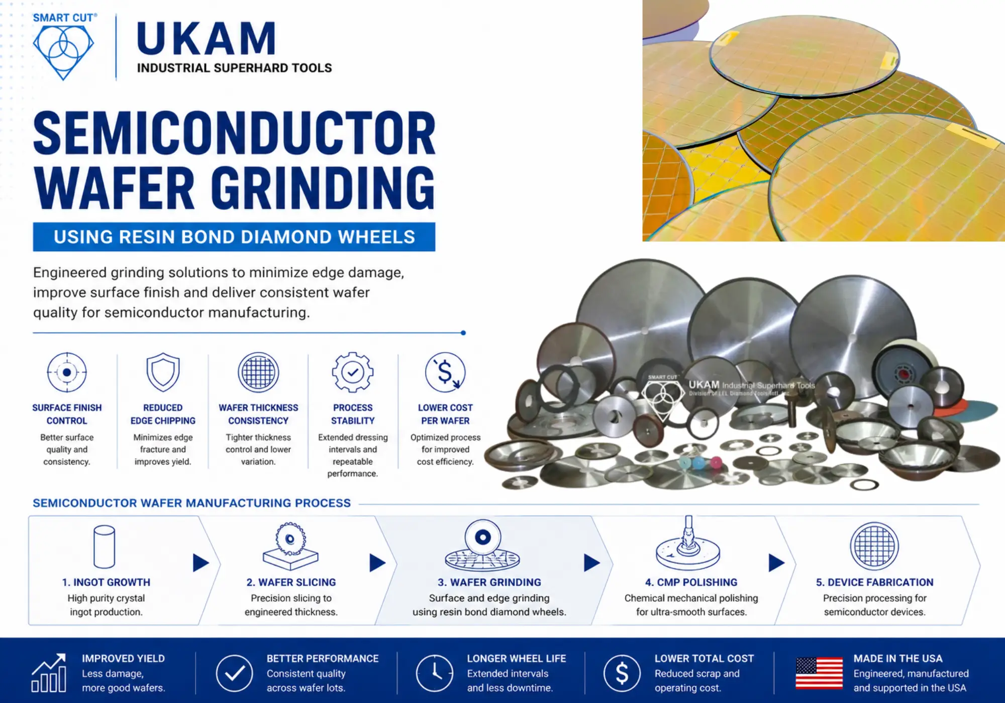
Table of Contents
Toggle
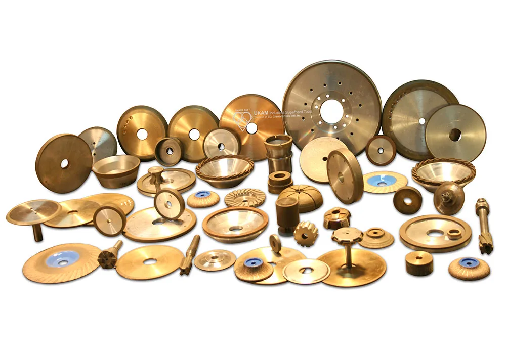
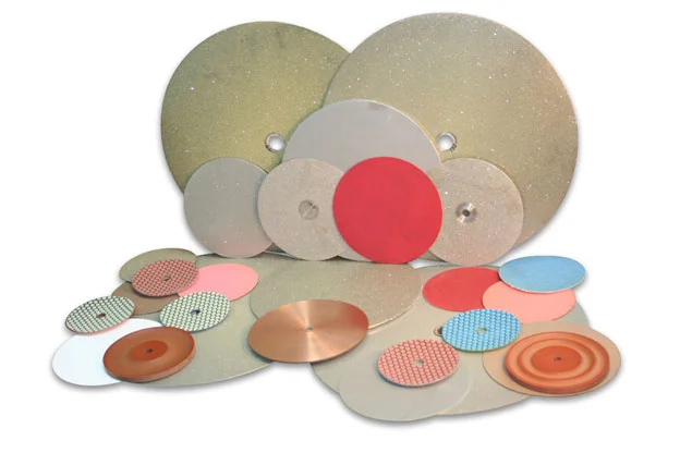
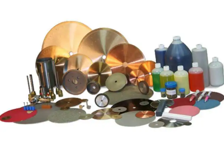
American Based Manufacturer

Established in 1990


Custom manufacturing


How a switch from metal bond to fine-grit resin bond diamond wheels, combined with standardized dressing intervals and revised finish-pass parameters, cut wafer edge chipping by ~60% while improving surface finish and lowering total cost per wafer.
Qualification Results Summary
|
Qualification Metric |
Original Process |
Optimized Process |
|---|---|---|
|
Edge Chipping Rate |
6.1% |
2.4% |
|
Surface Finish |
0.18 µm Ra |
Improved Consistency |
|
Dressing Interval |
Every 20 Wafers |
Every 45 Wafers |
|
Cycle Time |
4.8 min |
4.1 min |
|
Scrap Rate |
6.1% |
2.4% |
|
Cost Per Wafer |
$2.13 |
$1.61 |
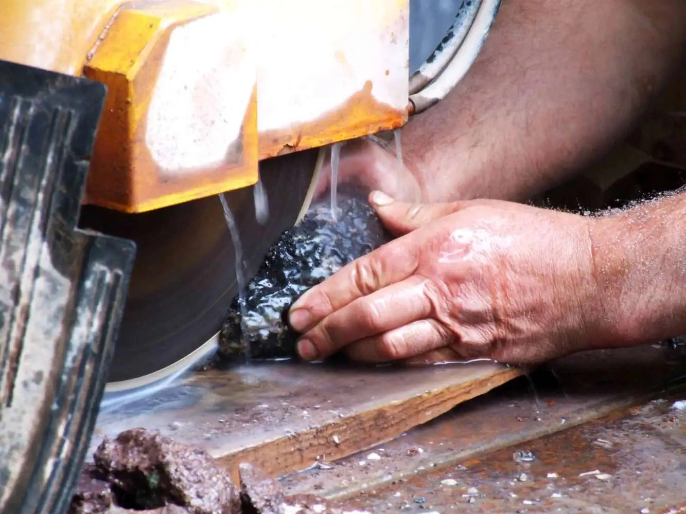
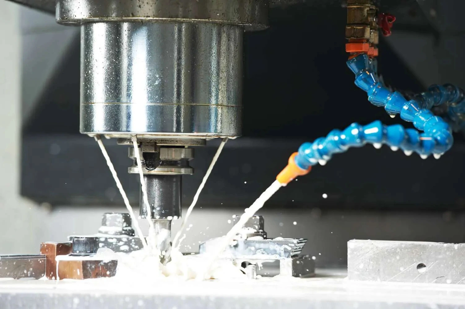
Edge chipping during semiconductor wafer grinding was generating unacceptable scrap rates on GaAs, sapphire, and silicon carbide substrates used in RF devices, power electronics, and optoelectronic manufacturing. The existing process used a metal bond diamond wheel optimized primarily for wheel life and dimensional retention. Production data showed progressive edge fracture, thermal haze, and subsurface cracking during finish grinding passes.
The failure mechanism was not isolated to a single variable. Grinding force increased as the wheel loaded. Dressing intervals varied between operators. Coolant delivery at the grinding zone dropped below the required flow rate during extended production runs. The combination created unstable grinding conditions that amplified brittle fracture at wafer edges.
Replacing the metal bond wheel with a fine-grit resin bond diamond wheel, combined with standardized dressing intervals and revised finish pass parameters, reduced wafer edge chipping by approximately 60% while improving surface finish consistency and lowering total cost per wafer.
Why Semiconductor Manufacturers Reevaluate Grinding Wheel Specifications

Grinding wheel specification reviews are typically triggered by measurable process instability rather than immediate catastrophic failure. Semiconductor grinding processes often degrade gradually over weeks of production.
|
Production Trigger |
What It Signals |
Engineering Response |
|---|---|---|
|
Increasing edge chipping |
Excess grinding force or wheel loading |
Review bond structure and dressing frequency |
|
Surface haze after finish grinding |
Thermal damage |
Reduce grinding energy and verify coolant flow |
|
Variation between operators |
Inconsistent dressing practice |
Standardize dressing intervals |
|
Increased spindle load |
Dull abrasive exposure |
Inspect wheel condition |
|
Random wafer breakout |
Vibration or unstable feed pressure |
Verify spindle runout and machine rigidity |
|
Scrap rate above 3% |
Process instability |
Conduct baseline qualification review |
|
Longer cycle times |
Reduced wheel cutting efficiency |
Evaluate self-sharpening behavior |
Brittle semiconductor materials behave differently than structural ceramics or tungsten carbide. Silicon carbide, sapphire, gallium arsenide, fused silica, and indium phosphide exhibit rapid crack propagation once localized stress exceeds the material fracture threshold.
Baseline Documentation Before Process Changes
No grinding trial should begin without baseline process data. Simultaneous changes to wheel bond, feed rate, spindle speed, and coolant flow prevent accurate root-cause analysis.
|
Parameter |
Measurement Method |
Unit |
Notes |
|---|---|---|---|
|
Wafer material |
Incoming inspection |
Material grade |
SiC, sapphire, GaAs, InP |
|
Wafer thickness |
Digital micrometer |
mm |
Record lot variation |
|
Wheel specification |
Supplier documentation |
Bond and grit |
Verify concentration |
|
Spindle speed |
Tachometer |
RPM |
Confirm actual speed |
|
Surface speed |
Calculated |
SFM |
Primary grinding parameter |
|
Feed rate |
CNC verification |
mm/min |
Separate rough and finish values |
|
Coolant flow at nozzle |
Flow meter |
L/min |
Do not measure at pump |
|
Coolant pressure |
Inline gauge |
PSI |
Verify consistency |
|
Dressing interval |
Production log |
Wafers per dress |
Record by operator |
|
Surface finish |
Profilometer |
Ra µm |
Compare before and after |
|
Edge chipping rate |
Optical inspection |
% rejected wafers |
Primary KPI |
|
Spindle runout |
Dial indicator |
Inches |
Critical for brittle materials |
The production audit showed that coolant flow measured at the nozzle was approximately 24% lower than the value measured at the pump due to restriction in the delivery system. Spindle runout also exceeded 0.00025 inches during extended operation.
Representative Wheel Variables Evaluated During Qualification
Although wheel specifications vary based on wafer material, machine configuration, and production objectives, the following variables were evaluated during process qualification
|
Parameter |
Engineering Consideration |
|---|---|
|
Bond Type |
Influences grinding force and wheel loading |
|
Diamond Grit Size |
Influences surface finish and edge quality |
|
Diamond Concentration |
Influences wheel life and grinding aggressiveness |
|
Wheel Diameter |
Influences surface speed and energy input |
|
Surface Speed |
Influences heat generation |
|
Coolant Method |
Influences thermal control |
|
Dressing Strategy |
Influences abrasive exposure consistency |
Actual wheel dimensions, grit designations, concentrations, and operating parameters vary by application.
Existing Process Conditions
The original process used a medium grit metal bond wheel for both rough and finish grinding. Operators selected dressing intervals based on audible spindle load changes rather than documented process controls.
Existing Production Conditions
|
Parameter |
Original Process |
|---|---|
|
Bond type |
Metal bond |
|
Grit size |
Medium |
|
Dressing interval |
Variable |
|
Finish feed rate |
Aggressive |
|
Coolant delivery |
Flood coolant only |
|
Wheel loading tendency |
High |
|
Edge chipping rate |
6.1% |
|
Average surface finish |
0.18 µm Ra |
The wheel retained dimensional accuracy well during rough grinding but generated progressively higher grinding forces during finish passes. Edge fracture occurred most frequently during spark-out and wafer exit transitions.
Cost Per Part Analysis: Metal Bond vs Resin Bond
Wheel price alone does not determine grinding economics. Scrap rate, dressing frequency, wheel life, cycle time, and process stability determine the actual production cost.
Illustrative Semiconductor Grinding Comparison
|
Parameter |
Metal Bond Whee |
Resin Bond Wheel |
|---|---|---|
|
Wheel price |
$680 |
$820 |
|
Wafers processed per wheel |
320 |
510 |
|
Dress interval |
Every 20 wafers |
Every 45 wafers |
|
Average cycle time |
4.8 min |
4.1 min |
|
Surface finish consistency |
Moderate |
High |
|
Scrap rate |
6.1% |
2.4% |
|
Cost per wafer from wheel cost |
$2.13 |
$1.61 |
|
Estimated scrap loss per 1,000 wafers |
$4,880 |
$1,920 |
|
Total estimated savings per 1,000 wafers |
Baseline |
Approx. $3,500 |
Illustrative values based on semiconductor wafer grinding environments. Actual results vary depending on substrate material, wheel specification, coolant system performance, and machine condition.
Most of the savings came from improved wafer yield rather than wheel longevity alone.
Ready to calculate savings for your substrate? Request a wheel specification →
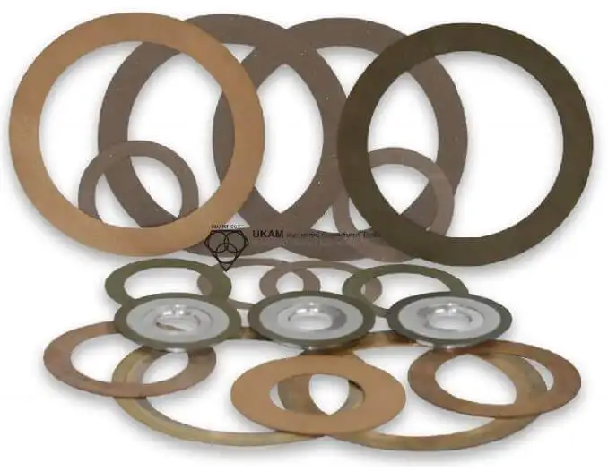
Bond Selection Reference Table

Bond structure determines wheel behavior under grinding pressure. Semiconductor finish grinding requires stable abrasive exposure with lower grinding energy.
|
Bond Type |
Self Sharpening |
Thermal Behavior |
Form Retention |
Best Application |
|---|---|---|---|---|
|
High |
Low heat generation |
Moderate |
Finish grinding of brittle wafers |
|
|
Low |
Higher grinding energy |
Very high |
Rough stock removal |
|
|
Controlled |
Stable thermal behavior |
High |
Precision ceramic grinding |
|
|
None |
Moderate |
Fixed geometry |
Profiling applications |
|
|
Moderate |
Controlled |
High |
Combined rough and finish applications |
The resin bond wheel selected during qualification used a finer grit specification with reduced diamond concentration to lower force concentration near wafer edges.
Grinding Wheel Variables Affecting Edge Chipping

Multiple wheel variables influence grinding force, heat generation, abrasive exposure, and edge integrity.
|
Variable |
Primary Influence |
|---|---|
|
Bond type |
Grinding force and wheel loading |
|
Diamond Grit Size |
Surface finish and edge quality |
|
Diamond Concentration |
Tool life and process stability |
|
Surface Speed |
Thermal generation |
|
Coolant Delivery |
Heat evacuation |
|
Dressing Frequency |
Abrasive exposure consistency |
|
Machine Rigidity |
Vibration control |
Diamond Grit Selection Considerations
|
Grit Category |
Typical Outcome |
|---|---|
|
Coarse |
Higher stock removal |
|
Medium |
Balanced performance |
|
Fine |
Improved surface finish |
|
Very Fine |
Precision finishing |
Diamond Concentration Selection Considerations
|
Concentration Level |
Typical Outcome |
|---|---|
|
Lower |
Faster cutting and shorter wheel life |
|
Medium |
Balanced performance |
|
Higher |
Longer wheel life and improved stability |
Coolant Delivery Considerations
|
Coolant Variable |
Engineering Impact |
|---|---|
|
Flow Rate |
Heat removal |
|
Pressure |
Coolant penetration |
|
Nozzle Position |
Cooling effectiveness |
|
Filtration |
Surface finish consistency |
|
Delivery Method |
Process stability |
These variables should be evaluated together during qualification rather than independently.
Step-by-Step Process Optimization
Phase 1 — Machine Qualification
Inspect spindle runout using a calibrated dial indicator. Semiconductor wafer grinding should maintain spindle runout below 0.0002 inches for brittle materials such as sapphire and GaAs. Verify machine rigidity during finish passes. Vibration amplification at high spindle speed directly contributes to edge fracture.
Phase 2 — Coolant Verification
Phase 3 — Wheel Selection
Phase 4 — Dressing Standardization
Phase 5 — Feed Rate Optimization
Phase 6 — Process Validation
Inspect wafers under magnification after each qualification lot. Track edge fracture frequency by material type. Measure surface finish and subsurface damage after polishing. UKAM’s consulting & process development team can support on-site qualification.
Need on-site process support? Contact UKAM’s engineering team →
Material-Specific Grinding Behavior
Silicon Carbide Wafers
Silicon carbide generates severe abrasive wear and wheel loading. The primary failure mode is thermal fracture caused by excessive grinding force after wheel dulling.
|
Material |
Failure Mode |
Recommended Bond |
|---|---|---|
|
Silicon Carbide |
Thermal fracture and wheel loading |
Fine grit resin bond |
Sapphire Substrates
Sapphire exhibits high hardness and low fracture tolerance during finish grinding. The primary failure mode is subsurface micro cracking near wafer edges.
|
Material |
Failure Mode |
Recommended Bond |
|---|---|---|
|
Sapphire |
Subsurface edge cracking |
Resin or vitrified bond |
Gallium Arsenide
GaAs wafers are highly sensitive to vibration and thermal stress. The primary failure mode is edge cleaving during spark-out.
|
Material |
Failure Mode |
Recommended Bond |
|---|---|---|
|
Gallium Arsenide (GaAs) |
Edge cleaving |
Fine grit resin bond |
Indium Phosphide
|
Material |
Failure Mode |
Recommended Bond |
|---|---|---|
|
Indium Phosphide |
Corner breakout |
Fine grit resin bond |
Fused Silica
|
Material |
Failure Mode |
Recommended Bond |
|---|---|---|
|
Fused Silica |
Thermal edge breakout |
Resin bond with controlled feed rate |
Working with a different substrate? Explore all semiconductor industry solutions →
Common Causes of Persistent Edge Chipping
|
Symptom |
Likely Cause |
Corrective Action |
|---|---|---|
|
Random edge fractures |
Spindle vibration |
Verify spindle runout |
|
Chipping after dressing |
Excessive dressing pressure |
Reduce dress depth |
|
Thermal haze |
Insufficient coolant flow |
Increase flow and pressure |
|
Localized breakout |
Feed pressure too high |
Reduce finish feed |
|
Increased spindle load |
Wheel loading |
Shorten dressing interval |
|
Surface scratching |
Grit contamination |
Replace coolant filtration |
|
Wafer cracking during spark-out |
Excess spark-out pressure |
Reduce finishing pressure |
Supplier Evaluation Table
Wheel consistency varies significantly between suppliers. Bond chemistry, wheel balancing, and abrasive retention directly affect semiconductor process stability.
|
Question to Ask |
What the Answer Reveals |
|---|---|
|
What bond structure is recommended for GaAs and sapphire? |
Indicates application engineering capability |
|
What dressing interval is recommended and why? |
Demonstrates process knowledge |
|
What balancing tolerance is maintained? |
Predicts vibration stability |
|
Can separate wheel specs be recommended for rough and finish passes? |
Shows semiconductor grinding experience |
|
What spindle speeds were used during qualification testing? |
Verifies real process validation |
|
How is wheel porosity controlled? |
Indicates coolant access consistency |
|
Can process optimization support be provided during qualification? |
Separates engineering suppliers from catalog resellers |
Suppliers unable to discuss spindle condition, coolant flow, dressing strategy, or grinding energy generally lack semiconductor wafer grinding experience. Learn more about UKAM’s process development and engineering consultation services.
SMART CUT® Technology Comparison
|
Parameter |
Conventional Metal Bond |
SMART CUT® Resin Bond |
|---|---|---|
|
Grinding force |
Higher |
Lower |
|
Wheel loading tendency |
Higher |
Lower |
|
Dressing frequency |
More frequent |
Less frequent |
|
Surface finish stability |
Variable |
More consistent |
|
Edge chipping tendency |
Moderate to high |
Lower |
|
Thermal loading |
Higher |
Reduced |
|
Finish pass stability |
Moderate |
Improved |
|
Wafer yield consistency |
Variable |
More repeatable |
The qualification results demonstrated that lower grinding force produced better edge integrity than maximizing wheel hardness or wheel retention. Read more about SMART CUT® Technology and how it redefines abrasive performance standards.
Qualification Checklist
Machine Condition
- Verify spindle runout below 0.0002 inches
- Confirm machine rigidity during finish passes
- Inspect spindle bearings
- Verify spindle speed accuracy
Coolant System
- Measure coolant flow at nozzle
- Verify coolant pressure stability
- Verify coolant pressure stability
- Inspect filtration system condition
Wheel Qualification
- Verify wheel balance certification
- Confirm grit size and concentration — see diamond concentration guide
- Record wheel wear during qualification
- Validate dressing interval consistency
Process Parameters
- Record separate rough and finish feed rates
- Track spindle load continuously
- Measure surface finish after each lot
- Record scrap rate by shift
Inspection Controls
- Inspect edge fracture under magnification
- Measure subsurface damage
- Compare before-and-after wafer yield
- Document thermal damage observations
Frequently Asked Questions
The resin bond wheel generated lower grinding forces because the bond released dull abrasive particles more easily during grinding. This reduced localized stress concentration at wafer edges. The metal bond wheel maintained dimensional retention longer, but grinding energy increased significantly once wheel loading developed.
Semiconductor wafers fracture under relatively small vibration spikes. Spindle runout amplifies localized grinding force at the wafer edge. GaAs and sapphire substrates are particularly sensitive to vibration-induced fracture during finish passes.
Operators previously dressed the wheel based on sound and spindle feel rather than measured process data. Wheel loading developed differently across shifts. Standardized dressing intervals stabilized abrasive exposure and reduced variation between operators. Rotary diamond dressers help maintain consistent dressing geometry across all shifts.
Pump output does not represent actual coolant delivery at the grinding interface. Hose bends, nozzle geometry, and partial restrictions reduce flow substantially. Reduced coolant delivery increased localized heat generation near wafer edges.
Rough grinding prioritizes material removal rate and dimensional control. Finish grinding prioritizes edge integrity and surface finish. Using a single aggressive parameter set for both stages generated excessive grinding force during finish passes.
Vitrified bond wheels perform well in many ceramic grinding applications and certain semiconductor processes. In this qualification study, the resin bond wheel produced lower grinding energy and improved edge integrity on brittle substrates such as GaAs and sapphire.
The largest improvement came from stabilizing grinding force during finish passes. Lower grinding energy, consistent dressing intervals, improved coolant delivery, and reduced spindle vibration collectively reduced edge fracture and thermal damage.
Key Engineering Principles
- Semiconductor wafer grinding failures are primarily force and thermal management problems.
- Wheel specification directly affects grinding energy and edge integrity.
- Resin bond wheels reduce grinding force through controlled abrasive release.
- Dressing intervals must be standardized across all production shifts using rotary diamond dressers.
- Coolant flow must be measured at the grinding zone rather than the pump.
- Spindle runout directly affects brittle semiconductor substrates.
- Surface finish and edge quality require separate optimization from rough stock removal.
- Scrap reduction often generates larger savings than maximizing wheel life.
- Stable wafer grinding depends on balancing wheel specification, coolant delivery, spindle condition, and feed rate together.
- Semiconductor grinding processes should be validated separately for each substrate material family — explore UKAM’s full range of semiconductor industry solutions.
Trusted by Tens of Thousands of Manufacturers, Laboratories,
Research Institutions Worldwide Since 1990
American Based Manufacturer
Established in 1990
Custom manufacturing
RELATED ARTICLES