






























Semiconductor Wafer Edge Inspection: Defect Classification, Measurement, and Acceptance Criteria

Table of Contents
Toggle
American Based Manufacturer

Established in 1990


Custom manufacturing


Semiconductor wafer edge inspection is an important part of process quality control because defects around the wafer perimeter can affect subsequent handling, processing, and wafer integrity. Chips, cracks, scratches, and edge-profile deviations must be identified consistently before engineers can determine whether a wafer meets the applicable requirements.
A useful inspection process does more than identify visible damage. It establishes where a defect occurs, how it is measured, which inspection method was used, and whether the result meets the approved acceptance criteria.
For process engineers, quality engineers, and manufacturing teams, the objective is to make inspection results repeatable, traceable, and suitable for process investigation.
This guide explains how to classify semiconductor wafer edge defects, select inspection methods, measure defects consistently, establish specification-based acceptance criteria, and document findings for corrective action.
Why Semiconductor Wafer Edge Inspection Matters

The wafer edge is exposed to mechanical contact during several manufacturing and handling operations. Depending on the process sequence, inspection may be required after edge profiling, grinding, dicing, polishing, cleaning, or wafer handling.
Inspection helps engineering teams:
- Identify edge defects before the next manufacturing operation.
- Distinguish visible surface damage from suspected cracking or profile deviations.
- Compare defect occurrence across machines, fixtures, process stages, and production lots.
- Determine whether a wafer meets the applicable drawing, customer specification, or internal control plan.
- Establish a documented baseline for investigating changes in defect frequency or severity.
Inspection findings should be interpreted in the context of the wafer material, edge geometry, process stage, and inspection capability. A defect observed after one operation cannot automatically be attributed to that operation without supporting evidence.
Classification of Wafer Edge Defects
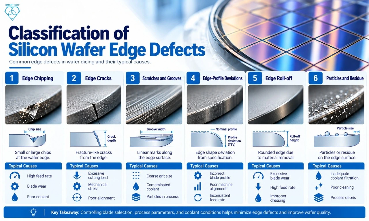
A consistent classification system prevents different operators from recording the same defect in different ways.
Edge chipping
Edge chipping refers to a localized loss of material from the wafer edge. A chip may appear as a small notch, a larger missing section, or an irregular discontinuity along the perimeter.
Record the chip’s location, visible dimensions, inspection method, and relationship to the defined edge geometry. A two-dimensional image can establish visible lateral dimensions, but it does not necessarily establish the full three-dimensional extent of the damage.
Edge cracks
Cracks are fracture-like discontinuities that may extend from the edge into the wafer. They should be distinguished from chips because the visible opening of a crack may not represent its full extent.
Where crack depth or subsurface extension affects disposition, use a suitable validated inspection or evaluation method. Do not infer crack depth from surface appearance alone.
Scratches and grooves
Scratches and grooves are elongated surface features. Record their orientation, location, and measurable dimensions where the inspection method supports those measurements.
A surface mark should not be classified as a crack without adequate evidence.
Edge-profile deviations
These include deviations in the specified edge radius, bevel, chamfer, or other defined edge geometry. Assessment requires a suitable dimensional or profile measurement method and a reference specification.
Edge roll-off
Edge roll-off is a change in surface profile near the wafer perimeter. Its significance depends on the relevant process, measurement location, and applicable geometry or flatness requirements. It should not be assessed solely from a photograph of the wafer edge.
Particles and residue
Particles, contamination, or residue may be visible near the edge. Record their observed location and appearance, and use an appropriate method if material identification or contamination analysis is necessary.
Recommended inspection codes
The following codes are a proposed internal convention, not a universal semiconductor industry standard.
|
Code |
Defect category |
Primary record |
|---|---|---|
|
EC |
Edge chip |
Location and visible chip dimensions |
|
CR |
Crack |
Location and validated crack assessment |
|
SG |
Scratch or groove |
Orientation and measurable dimensions |
|
EP |
Edge-profile deviation |
Profile measurement against specification |
|
ER |
Edge roll-off |
Profile data and measurement location |
|
PT |
Particle or residue |
Location and appropriate contamination assessment |
|
UN |
Unclassified indication |
Image, location, and further evaluation required |
Organizations should define their own classification rules, image examples, and escalation requirements in the applicable inspection procedure.
Selecting the Appropriate Inspection Method
The inspection method must match the defect being evaluated. A method suitable for detecting visible surface chips may not be sufficient for measuring edge geometry or evaluating subsurface damage.
Optical inspection
Optical inspection is useful for identifying visible chips, scratches, particles, and other surface indications. Results depend on illumination, magnification, contrast, focus, surface condition, and the instrument’s detection capability.
Use controlled imaging conditions when comparing inspection results between wafers, operators, or production lots.
Microscopy
Microscopy can provide greater detail for evaluating small visible features and distinguishing their morphology. However, magnification alone does not establish measurement accuracy or prove that a feature extends below the surface.
The selected optical setup, calibration status, resolution, and measurement procedure should be appropriate for the feature size and required decision.
Automated edge inspection
Automated systems can support consistent inspection over defined wafer-edge regions and can help generate defect-location maps. Their performance depends on system configuration, detection settings, wafer presentation, and the defect types represented during validation.
Before using automated results for acceptance decisions, establish that the system can detect and classify the defects relevant to the application.
Edge-profile and dimensional metrology
Profile measurement is appropriate when the requirement concerns edge radius, bevel geometry, dimensional conformity, or surface profile.
Use the relevant drawing or specification to establish the measurement locations, reference geometry, and permitted deviations. A surface image alone is not a substitute for dimensional metrology when a profile tolerance applies.
Subsurface damage evaluation
Where the engineering requirement concerns damage beneath the visible surface, a surface-only inspection may be insufficient. The appropriate evaluation method depends on the material, suspected damage mechanism, required detection depth, and available validated procedure.
Document the method and its limitations. Do not report subsurface damage as confirmed unless the method supports that conclusion.
How to Measure Edge Defects Consistently
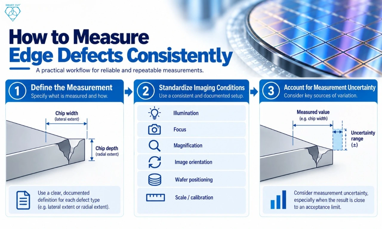
Measurement consistency is essential when defect dimensions are used to accept a wafer, reject it, or initiate a process investigation.
Define the measurement before collecting data
For a visible edge chip, the procedure should define the reported dimension. Depending on the application, this might be the maximum visible lateral extent, radial extent from a specified edge reference, or another clearly defined geometric measurement.
These measurements are not interchangeable. The chosen definition must match the applicable acceptance requirement.
For cracks, define the measurement endpoint and the method used to establish it. For profile deviations, identify the reference geometry and measurement location.
Standardize imaging conditions
Use a documented procedure for illumination, focus, magnification, image orientation, and wafer positioning. Include a suitable scale or calibrated measurement reference when dimensional results are required.
Where possible, retain the original image alongside any annotated measurement. This allows another engineer to review the observation without relying solely on the recorded number.
Account for measurement uncertainty
Every measurement has limitations. Sources may include instrument calibration, image resolution, edge contrast, focus, operator selection of defect boundaries, and the repeatability of the measurement procedure.
The uncertainty associated with a reported dimension should be considered when the result is close to an acceptance limit.
Illustrative example, not a universal wafer acceptance rule:
Assume an approved specification permits a maximum measured chip dimension of 40 µm under a defined measurement procedure. An inspection result is 38 µm, with an estimated expanded measurement uncertainty of ±4 µm.
The result is close enough to the limit that the measurement uncertainty could affect the disposition. The engineer should follow the organization’s documented decision rule, which may require a more capable measurement, a repeat measurement, or review by the responsible quality authority.
The result should not automatically be declared acceptable simply because the displayed value is below 40 µm. Nor should uncertainty automatically mean rejection. The decision must follow the agreed specification and decision rule.
Record what the inspection method actually shows before assigning a suspected cause.
For example:
- Observation: A localized chip is visible at the wafer perimeter.
- Measurement: The maximum visible lateral extent is recorded using the defined imaging procedure.
- Interpretation: The morphology may be consistent with mechanical contact or process-related damage.
- Confirmation: A cause is assigned only after supporting evidence is evaluated.
Establishing Wafer Edge Acceptance Criteria
There is no single chip-size limit that can be applied to every semiconductor wafer. Acceptance requirements depend on the wafer material, edge geometry, device or process requirements, manufacturing stage, customer specification, and approved inspection method.
An acceptance procedure should define the following:
|
Requirement |
What the procedure should specify |
|---|---|
|
Defect category |
Which defect types are evaluated |
|
Measurement definition |
How each reported dimension is determined |
|
Inspection coverage |
Which edge regions and surfaces are examined |
|
Detection capability |
Which defect sizes or characteristics the method can reliably detect |
|
Acceptance limit |
The applicable drawing, customer, or internal limit |
|
Decision rule |
How measurement uncertainty and borderline results are handled |
|
Disposition |
Accept, reject, hold, or escalate under defined conditions |
|
Traceability |
How results are linked to the wafer, lot, process stage, and inspection record |
The specification should identify the applicable revision and authority. If a limit is missing, ambiguous, or inconsistent with the measurement method, the engineer should seek clarification rather than invent a threshold.
Sampling requirements must also be defined. Inspection of selected wafers cannot automatically establish that every wafer in a lot is free from edge defects. Sampling plans should reflect the process risk, defect history, applicable quality requirements, and purpose of the inspection.
Validating the Inspection and Measurement System
A consistent-looking result is not necessarily an accurate or sufficiently sensitive result. Before inspection data are used for process control or product disposition, evaluate the measurement system for its intended purpose.
Calibration and traceability
Confirm that relevant instruments are within their calibration requirements and that dimensional measurements are traceable as required by the organization’s quality system.
Calibration alone does not establish that the complete inspection procedure is suitable for every defect type.
Repeatability
Repeatability evaluates the variation observed when the same operator measures the same feature using the same method and equipment under comparable conditions.
Large variation may indicate inconsistent defect-boundary selection, unstable imaging conditions, insufficient resolution, or an inadequately defined procedure.
Reproducibility
Reproducibility evaluates differences associated with factors such as operators, instruments, or measurement setups. If multiple operators produce materially different results, the procedure may need clearer measurement definitions, training, or improved instrumentation.
Detection capability
Determine whether the inspection system can reliably detect the defect types and sizes relevant to the acceptance criteria. A system may produce highly repeatable measurements for defects it detects while failing to detect smaller or lower-contrast defects.
Where appropriate, validate detection performance using representative samples or suitable reference artifacts, with a documented method and defined limitations.
The validation plan should be proportionate to the risk and intended use of the inspection system.
Recording Results and Mapping Defect Locations
An inspection record should allow another engineer to understand what was observed, how it was measured, and why the disposition was made.
Recommended inspection record
Record the following information where applicable:
- Wafer or sample ID, material, dimensions, and lot number.
- Process stage, machine or equipment ID, and inspection date.
- Defect classification and location using a defined wafer reference.
- Measurement definition, measured value, unit, and uncertainty where relevant.
- Inspection instrument, method, calibration status, and detection limitations.
- Original image or profile data, with annotations where appropriate.
- Applicable specification and revision.
- Acceptance decision, decision rule, and reviewer.
- Suspected cause, supporting evidence, corrective action, and verification result.
Illustrative inspection record
The following entry is hypothetical and is not UKAM production data.
|
Field |
Example entry |
|---|---|
|
Sample ID |
DEMO-001 |
|
Material |
Silicon |
|
Inspection stage |
After edge finishing |
|
Defect category |
Edge chip |
|
Location |
120° from the defined reference |
|
Measured feature |
Maximum visible lateral extent |
|
Recorded dimension |
35 µm |
|
Method |
Calibrated optical image |
|
Specification status |
Pending specification review |
|
Disposition |
Hold pending review |
The 35 µm value is an example measurement only, not an acceptance limit. The entry remains on hold because the applicable acceptance requirement and decision rule have not yet been confirmed.
Defect mapping
A defect map records where indications occur around the wafer perimeter. Use a consistent angular or positional reference so that results can be compared across inspection stages and production lots.
Repeated defects in a particular region may justify investigation of a localized contact point, fixture, handling step, or equipment condition. A spatial pattern is evidence for investigation, not proof of a cause.
Where process records are available, compare defect maps with equipment, handling, and process history before selecting a corrective action.
Using Inspection Results for Root-Cause Investigation
Inspection data become more useful when the investigation distinguishes defect detection from cause confirmation.
A practical investigation can follow this sequence:
- Confirm the indication. Verify that the feature is real and that the inspection method is appropriate for its classification.
- Verify the measurement. Repeat or independently review measurements when the result is borderline, inconsistent, or consequential.
- Compare process stages. Determine whether the defect was present before the operation under investigation or appeared afterward.
- Review process evidence. Examine relevant machine records, tool condition, fixture contact, handling procedures, and process settings.
- Form a testable hypothesis. Identify a plausible mechanism and the evidence that would support or contradict it.
- Implement a controlled change. Modify the relevant process variable only when the investigation supports that action.
- Verify the result. Use the defined inspection method and acceptance criteria to determine whether the corrective action produced the intended outcome.
For example, a chip observed after edge finishing should be compared with the available pre-process inspection record. If no baseline exists, the timing of defect formation may remain uncertain. That limitation should be documented rather than attributing the chip to the finishing operation without evidence.
Practical Inspection Checklist
Before releasing inspection results, confirm that:
- The wafer and inspection stage are identified.
- Defects are classified using the approved terminology.
- Measurement definitions and units are documented.
- The selected method is suitable for the defect being evaluated.
- Instrument calibration and relevant measurement limitations have been checked.
- Borderline measurements are handled using the approved decision rule.
- Acceptance limits come from the applicable specification.
- Defect locations and supporting images are retained where required.
- The disposition is traceable to the responsible reviewer.
- Any suspected cause is distinguished from a confirmed cause.
- Corrective actions are verified using defined criteria.
The Role of Precision Diamond Tooling
Inspection findings can help engineers evaluate whether an edge-processing operation requires further investigation. However, defect appearance alone cannot establish that a particular tool or bond type caused the damage.
Tool selection should be considered alongside the substrate material, required edge geometry, process conditions, machine setup, and the inspection evidence. Any change to tooling or process parameters should be evaluated through controlled trials and documented verification.
For information about UKAM’s semiconductor-related tooling range, see the UKAM Semiconductor Industry page. Product suitability should be confirmed against the actual material, operation, and required specification.
For broader manufacturing context, readers can also consult UKAM’s guide to semiconductor wafer cutting, grinding, dicing, and polishing.
Conclusion
Reliable semiconductor wafer edge inspection requires more than identifying visible chips. Engineers need consistent defect definitions, suitable inspection methods, documented measurement procedures, appropriate acceptance criteria, and traceable disposition records.
Measurement uncertainty and detection capability are particularly important when results are close to specification limits. By validating the inspection system and separating observations from suspected causes, manufacturing teams can make better-supported quality decisions and conduct more effective process investigations.
The goal is not simply to count edge defects. It is to produce inspection data that are repeatable, technically defensible, and useful for controlling manufacturing quality.
American Based Manufacturer
Established in 1990
