


Semiconductor Wafer Manufacturing Process: Cutting, Grinding, Dicing & Polishing Tools Explained
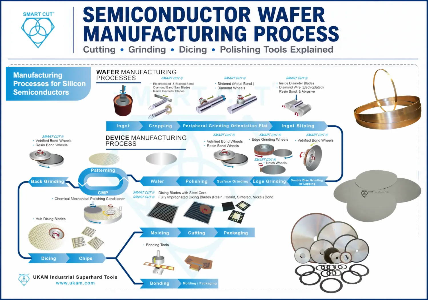
Table of Contents
ToggleModern semiconductor manufacturing demands extreme precision at every stage — from preparing a silicon ingot to singulating individual chips. Each operation directly shapes device performance, production yield, surface integrity, and cost per wafer. As chips become smaller, thinner, and more complex, the diamond tooling and abrasive consumables used throughout the process have become equally critical to the finished product as the semiconductor material itself.
This guide walks through the complete semiconductor wafer manufacturing process, with a sharp focus on the precision diamond tools used at each stage. Whether you are a process engineer, procurement specialist, or materials researcher, understanding the relationship between tooling selection and process outcomes is essential for improving quality and reducing scrap.
At UKAM Industrial Superhard Tools, we have spent over 40 years engineering and optimizing diamond tools for silicon, SiC, GaN, sapphire, and advanced ceramics. This article reflects real-world process knowledge accumulated across thousands of semiconductor fabrication applications.
Trusted by Tens of Thousands of Manufacturers, Laboratories Research Institutions Worldwide Since 1990

American Based Manufacturer

Established in 1990


Custom manufacturing


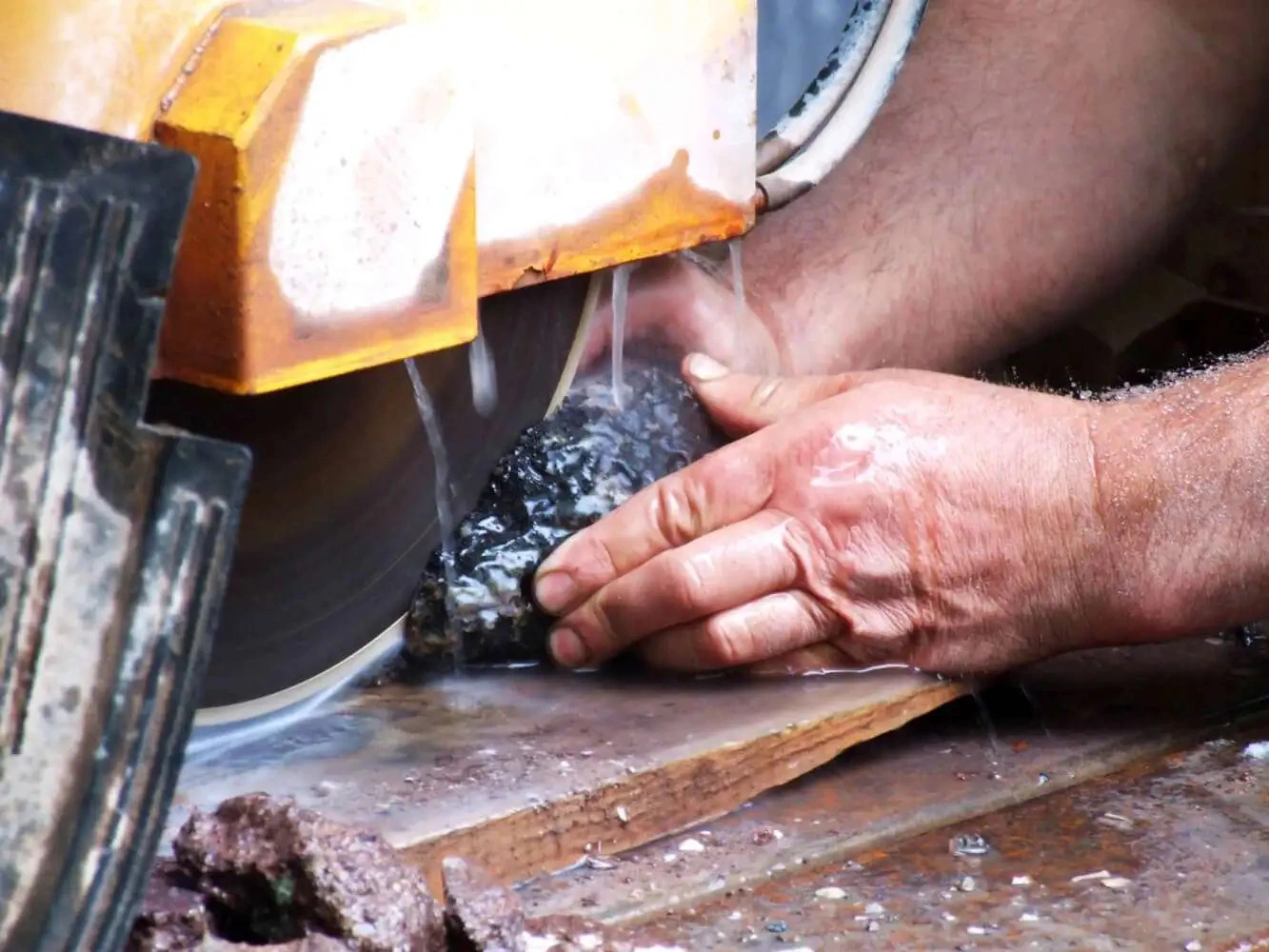
Stage 1: Ingot Preparation and Cropping
The semiconductor manufacturing process begins long before a wafer is formed. Raw silicon is grown into cylindrical ingots — either through the Czochralski (CZ) or Float Zone (FZ) method — and these ingots must be precisely prepared before slicing can begin. Cropping removes seed ends, tail sections, and zones with crystal defects, voids, or contamination that would compromise downstream yield.
Two primary tool families handle this stage: diamond band saw blades and ID (inside diameter) blades.

-
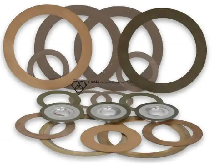
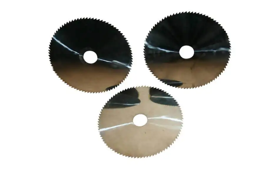
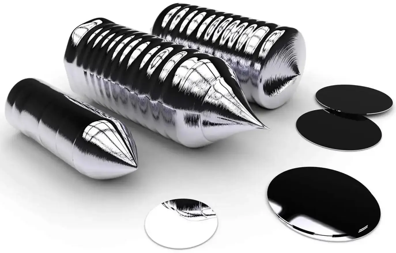
Diamond Band Saw Blades (Electroplated and Brazed Bond)
Diamond band saw blades operate in a continuous loop, providing stable cutting action with reduced vibration. Electroplated blades offer sharp, aggressive cutting ideal for silicon and ceramics, while brazed bond designs provide greater diamond retention for harder or more abrasive materials such as SiC and sapphire. Typical band saw blade speeds range from 800 to 2,500 m/min depending on material hardness and ingot diameter.
Key advantages include high material removal rate, ability to cut large-diameter ingots (200 mm to 300 mm+), low kerf loss versus conventional abrasive methods, and a continuous cutting action that minimizes localized stress. Water-based coolants with additives are required to control heat, prevent blade loading, and protect crystal integrity. -
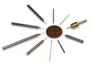
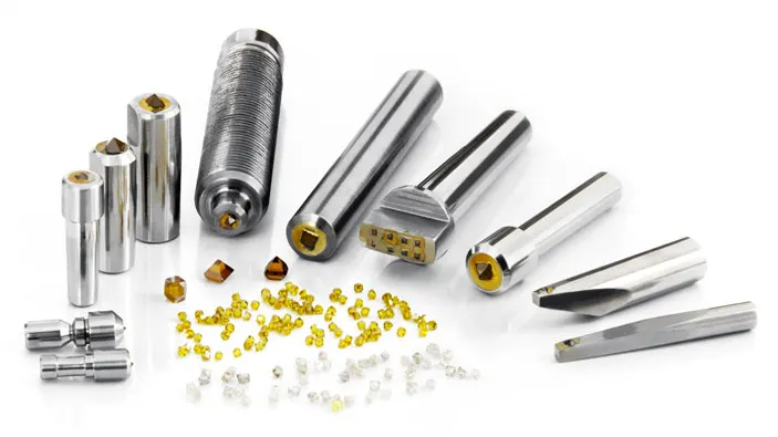
ID Blades (Inside Diameter Blades)
For high-value materials and applications requiring tighter tolerances, ID blades are the preferred cropping tool. The cutting action occurs on the inner edge of a thin, tensioned circular blade, providing exceptional stability, flatness, and parallelism. ID blades excel with smaller diameter ingots and materials such as GaAs, LiTaO3, and optical-grade sapphire where surface damage must be minimized even at the cropping stage.
Blade tension and RPM matching to blade diameter are critical parameters. Too little tension introduces deflection and taper; too much risks blade fracture.
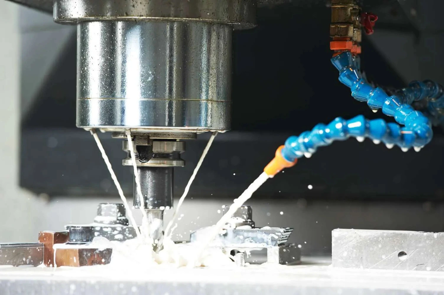
Stage 2: Wafer Formation — Peripheral Grinding and Ingot Slicing
Wafer formation converts the prepared ingot into individual wafers with defined thickness, flatness, and surface integrity. It involves two sequential operations: peripheral (OD) grinding and ingot slicing.

-
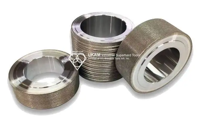
Peripheral Grinding and Orientation Feature Formation
Peripheral grinding brings the ingot to its precise target diameter and improves roundness before slicing. Sintered (metal bond) diamond wheels are the primary tool for bulk OD grinding, offering high rigidity, excellent shape retention, and long tool life. Typical ingot diameter tolerances after peripheral grinding are ±0.2 mm or better.
Orientation flats (for wafers 200 mm and below) or notches (for 300 mm wafers) are then formed using resin bond diamond wheels, which provide a smoother grinding action and reduce subsurface damage — critical because any damage introduced here can propagate into subsequent process steps. In automated high-precision systems, vitrified bond diamond wheels are increasingly used for their controlled porosity, superior coolant flow, and consistent cutting performance across long production runs. -
Ingot Slicing: ID Blades vs. Diamond Wire
Slicing converts the ingot into wafers with tight thickness tolerances (typically ±5 µm TTV for advanced applications) and minimal kerf loss. Two tool technologies dominate this stage:
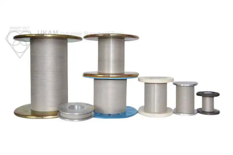
Diamond wire has become the dominant technology for large-diameter silicon ingots due to its very low kerf loss and ability to slice hundreds of wafers per run. Electroplated diamond wire diameters typically range from 80 µm to 160 µm; smaller wire reduces kerf loss but requires more precise tension control. ID blades remain preferred for high-value compound semiconductors and research applications where dimensional precision outweighs throughput.
UKAM offers precision ID blades and diamond wire optimized for silicon, SiC, GaAs, and sapphire slicing applications.
|
Parameter |
ID Blades |
Diamond Wire |
|---|---|---|
|
Throughput |
Lower (one cut at a time) |
High (multi-wire simultaneous) |
|
Kerf Loss |
~150–300 µm |
~100–180 µm |
|
Surface Damage |
Low, controlled |
Moderate, process-dependent |
|
Best For |
High-value, tight-tolerance wafers |
Large-diameter, high-volume production |
|
Material Range |
Si, SiC, GaAs, sapphire |
Silicon, solar, large ingots |
Stage 3: Wafer Finishing — Surface Grinding, Edge Grinding, and CMP

Wafer finishing transforms sliced wafers into geometrically accurate, device-ready substrates. At this stage, flatness, surface roughness, edge strength, and thickness uniformity must all meet specification simultaneously. The finishing sequence typically progresses through surface grinding, edge grinding, double-disc grinding or lapping, and CMP polishing.
-
Surface Grinding: The Three-Bond Progression
Surface grinding removes saw damage and achieves the target wafer thickness. Optimal results require a structured progression through three bond types- Metal bond (sintered) diamond wheels for bulk removal — highest rigidity, fastest removal rate, but greatest subsurface damage
- Vitrified bond diamond wheels for precision intermediate grinding — porous structure enables excellent coolant flow, high flatness control, and consistent geometry across production runs
- Resin bond diamond wheels for final surface preparation — softer bond action produces Ra values below 5 nm and minimizes subsurface damage depth before lapping or CMP
Skipping steps in this progression risks carrying forward damage that CMP cannot fully remove. Grit progression typically moves from 200–400 mesh (coarse/medium) for metal and vitrified stages down to 1200–3000 mesh or finer for resin bond finishing passes. -
Edge Grinding and Wafer Edge Profiling
Edge grinding — more precisely, edge profiling — shapes the wafer perimeter to prevent crack propagation and mechanical breakage during handling. Without proper edge rounding, stress concentrations at sharp edges cause yield losses during thermal cycling, spin coating, and robotic handling.
Resin bond diamond edge grinding wheels are the standard choice for this operation, creating controlled radius profiles (typically R = 0.2 mm to 0.5 mm) with minimal chipping. For orientation notch formation in 300 mm wafers, precision notch wheels with profiled geometries are required.
Fine grit (600–1200 mesh) wheels are used for finishing to achieve a smooth, chip-free edge surface.
Explore UKAM's diamond edge grinding wheels for silicon, SiC, and sapphire wafer edge profiling. -
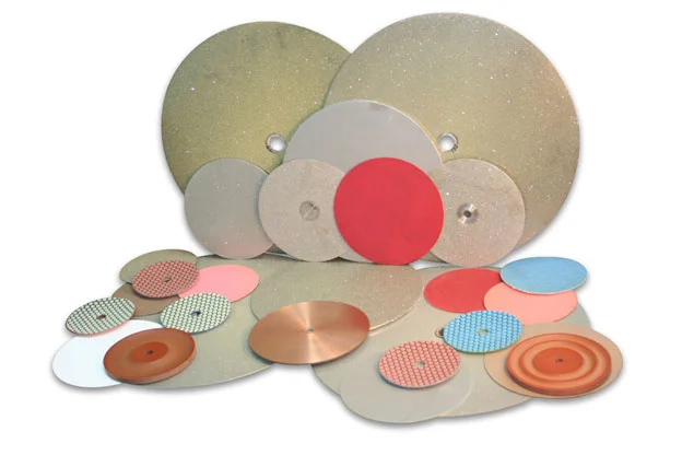
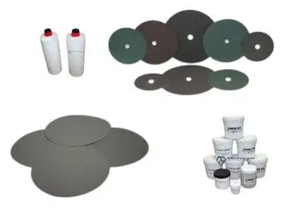
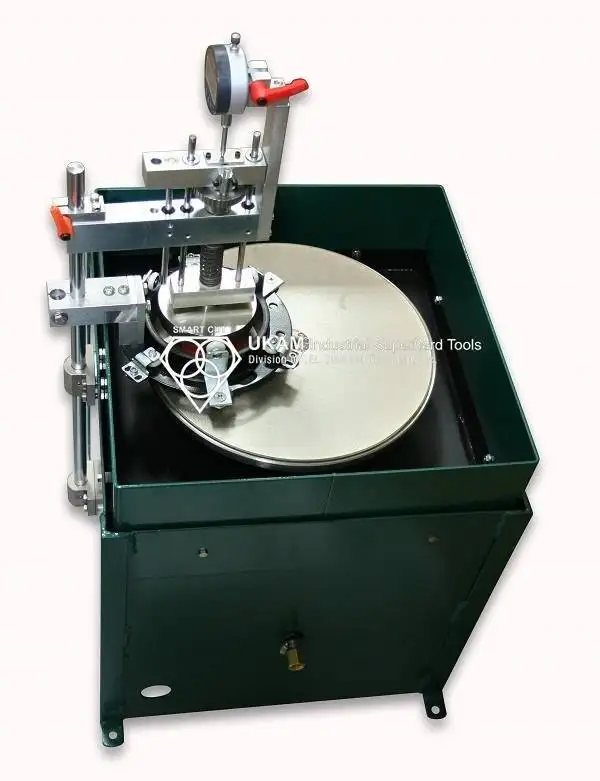
CMP — Chemical Mechanical Polishing
CMP is the final surface finishing step, achieving an atomically smooth wafer surface (Ra < 0.5 nm for prime-grade silicon) by combining chemical reactivity with controlled mechanical abrasion. The CMP system relies on four consumable components working in concert:<- CMP polishing pads — provide a controlled contact surface; hardness and groove geometry determine removal rate uniformity across the wafer
- Colloidal silica slurry — submicron abrasive particles in an alkaline or acidic chemistry selectively remove material at a rate of 100–300 nm/min for silicon
- Diamond CMP conditioning discs — maintain pad surface roughness (Rz typically 20–60 µm) to ensure consistent slurry transport and removal rate over the pad's lifetime
- DI water — used for dilution, cleaning, and preventing contamination between process steps
Without regular pad conditioning, glazing reduces removal rate and uniformity. Diamond conditioning discs embedded with precisely graded synthetic diamond are critical to CMP process stability and are often the single most underappreciated consumable in the CMP system.
UKAM manufactures diamond CMP conditioning discs for a wide range of pad types and polishing applications.
Stage 4: Device Manufacturing — Back Grinding and Wafer Dicing
Once front-side device fabrication is complete, wafers undergo back grinding and then dicing (singulation) to produce individual chips. These are among the most yield-sensitive operations in the entire process, because any tooling-induced defect at this stage directly affects finished device performance and reliability.
-
Back Grinding
Back grinding reduces wafer thickness to meet packaging requirements — commonly from 700 µm down to 50–100 µm or thinner for advanced packaging and 3D integration. The tool progression mirrors surface grinding: metal bond wheels for bulk removal, followed by fine resin bond wheels for the final pass to minimize subsurface damage on the thinned wafer. Hybrid bond wheels (combining sintered and resin bond characteristics) are increasingly used for advanced back grinding applications where both throughput and surface quality are critical.
Wafer warpage and TTV control become more demanding as target thickness decreases. Fine grit (2000–8000 mesh) resin bond wheels are often used for the final grinding pass on ultra-thin wafers (below 75 µm). -
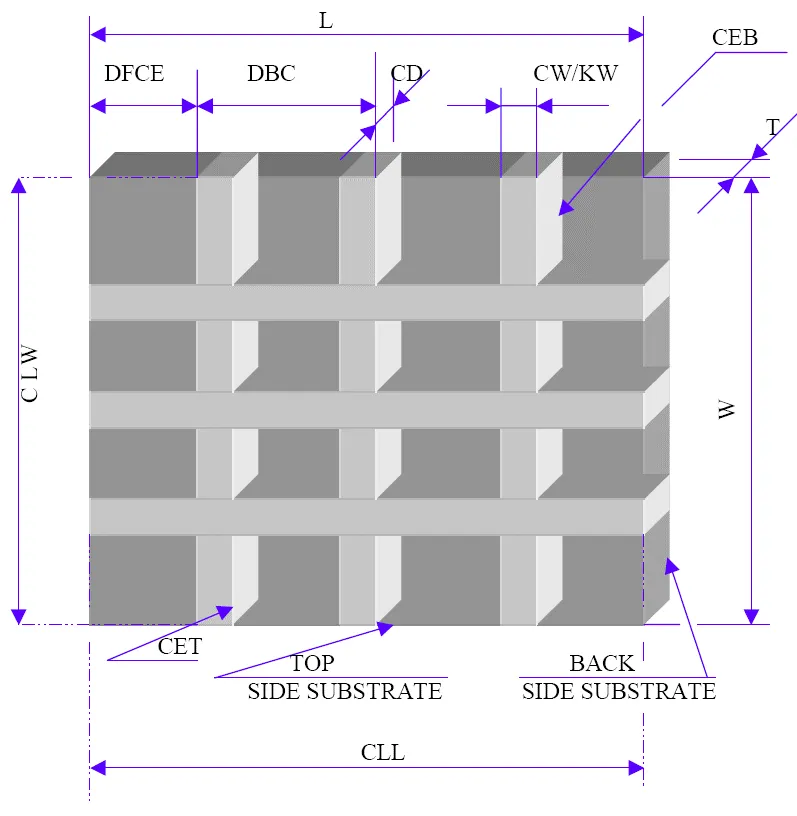
Wafer Dicing: Blade Selection by Application
Dicing separates the processed wafer into individual die along predefined streets. Blade selection at this stage has a direct and measurable impact on chipping width, die strength, and yield. Four blade bond types are used depending on material and application:
Hub dicing blades, where the blade is mounted on a rigid metal hub, are the standard for high-volume production because the hub provides superior rigidity, reduced vibration, and better cut depth consistency. Blade exposure (the amount of blade extending beyond the hub flange), RPM (typically 20,000–60,000 RPM), and feed rate must all be optimized together for each material and street width.
For advanced packaging applications where die must be singulated from molded panels or laminate substrates, diamond router bits and stealth dicing approaches are also used alongside conventional blade dicing.
Browse UKAM's full range of precision dicing blades for silicon, SiC, GaAs, and compound semiconductor applications.
|
Bond Type |
Kerf Thickness |
Best For |
Trade-Off |
|---|---|---|---|
|
Resin Bond |
15–50 µm |
Delicate Si, thin wafers, low chipping |
Shorter tool life |
|
Hybrid Bond |
20–75 µm |
Balance of speed and finish |
Moderate life and quality |
|
Sintered (Metal) |
50–150 µm |
Hard materials: SiC, sapphire |
Higher chipping risk if unoptimized |
|
Nickel (Electroplated) |
15–50 µm |
Fastest cutting speed, sharp action |
Shortest lifespan |
Semiconductor Diamond Tool Quick-Reference Guide
|
Process Stage |
Primary Tool |
Bond Type |
Key Parameter |
|---|---|---|---|
|
Ingot Cropping |
Band Saw Blades / ID Blades |
Electroplated / Metal |
Feed rate, coolant flow |
|
OD Grinding |
Sintered Diamond Wheels |
Metal Bond |
Grit size, wheel geometry |
|
Ingot Slicing |
ID Blades / Diamond Wire |
Metal / Electroplated |
Tension, RPM, kerf loss |
|
Surface Grinding |
Diamond Wheels (3-stage) |
Metal → Vitrified → Resin |
Grit progression, TTV |
|
Edge Grinding |
Edge / Notch Wheels |
Resin Bond |
Profile geometry, feed rate |
|
Lapping / DDG |
Diamond Wheels + Lapping Plates |
Metal / Abrasive Slurry |
Pressure, removal uniformity |
|
CMP Polishing |
Pads + Slurry + Conditioners |
Diamond Conditioning Disc |
Pad conditioning frequency |
|
Back Grinding |
Diamond Wheels |
Metal → Resin (fine) |
Thickness uniformity, warpage |
|
Wafer Dicing |
Dicing Blades / Hub Blades |
Resin / Hybrid / Metal / Ni |
Kerf width, RPM, chipping |
Frequently Asked Questions
Metal bond (sintered) diamond wheels offer the highest rigidity and longest tool life, making them ideal for bulk material removal and the initial grinding passes after ingot slicing. However, their hard bond retains worn diamond particles longer, which increases subsurface damage depth. Resin bond wheels have a softer matrix that allows worn particles to release more readily, producing a smoother cutting action with less subsurface damage and finer surface finish. For silicon wafer processing, the standard progression moves from metal bond to vitrified to resin bond to achieve both efficiency and surface quality.
Dicing blade bond hardness, diamond grit size, diamond concentration, and blade thickness all directly affect chipping width. Resin bond blades produce the lowest chipping (often below 5 µm on silicon) but wear faster. Metal bond blades last longer but may produce chipping of 10–30 µm or more if not optimized for the specific material. Grit size also matters: finer diamond produces smoother cuts with less chipping but requires higher spindle speed to maintain cutting efficiency. UKAM application engineers routinely help customers select blade specifications based on material, street width, and chipping tolerance requirements.
CMP pad conditioning is the process of mechanically refreshing the polishing pad surface during or between polish runs using a diamond-embedded conditioning disc. Over time, CMP pads glaze — the surface roughness decreases, slurry transport into the pad becomes less efficient, and removal rate drops non-uniformly across the wafer. Regular conditioning with a diamond disc restores the pad’s micro-texture, maintains stable removal rate, and prevents within-wafer non-uniformity. Conditioning disc specifications — including diamond grit size, concentration, and disc geometry — must be matched to the pad type and process targe
Silicon carbide (SiC) is one of the hardest semiconductor materials, with a Mohs hardness of approximately 9.5. Standard silicon wire saw and ID blade parameters are not adequate for SiC. Electroplated diamond wire with optimized diamond grit and wire tension, or ID blades with high-hardness metal bond and fine diamond, are the most common choices for SiC ingot slicing. Feed rates for SiC are typically 5–10x slower than for silicon, and coolant must be carefully managed to prevent thermal cracking. UKAM offers SiC-specific slicing solutions with bond and grit specifications developed through extensive application testing.
Kerf loss is the material consumed as waste during each cut, determined primarily by the cutting tool’s thickness. Diamond wire saw systems achieve the lowest kerf loss — typically 100–180 µm — compared to ID blade systems (150–300 µm) and conventional inner-hole saw blades. Reducing wire diameter reduces kerf, but thinner wire requires tighter tension control and is more susceptible to wire breakage. Process optimization, including feed rate, wire speed, and slurry concentration, also affects effective kerf loss in practice. For high-value materials such as SiC, minimizing kerf loss is particularly important given the cost of the ingot material itself.
UKAM supplies diamond tools for wafer processing across all common semiconductor wafer diameters, from 2-inch research wafers through 300 mm production wafers. Supported materials include silicon (monocrystalline and polycrystalline), SiC (4H and 6H), GaAs, GaN-on-silicon, InP, sapphire, LiTaO3, lithium niobate, quartz, and a range of advanced ceramics and optical crystals. Custom tool specifications are available for non-standard materials and applications. Contact UKAM at ukam.com to discuss your specific application requirements.
|
Process Stage |
Primary Tool |
Bond Type |
Key Parameter |
|---|---|---|---|
|
Ingot Cropping |
Band Saw Blades / ID Blades |
Electroplated / Metal |
Feed rate, coolant flow |
|
OD Grinding |
Sintered Diamond Wheels |
Metal Bond |
Grit size, wheel geometry |
|
Ingot Slicing |
ID Blades / Diamond Wire |
Metal / Electroplated |
Tension, RPM, kerf loss |
|
Surface Grinding |
Diamond Wheels (3-stage) |
Metal → Vitrified → Resin |
Grit progression, TTV |
|
Edge Grinding |
Edge / Notch Wheels |
Resin Bond |
Profile geometry, feed rate |
|
Lapping / DDG |
Diamond Wheels + Lapping Plates |
Metal / Abrasive Slurry |
Pressure, removal uniformity |
|
CMP Polishing |
Pads + Slurry + Conditioners |
Diamond Conditioning Disc |
Pad conditioning frequency |
|
Back Grinding |
Diamond Wheels |
Metal → Resin (fine) |
Thickness uniformity, warpage |
|
Wafer Dicing |
Dicing Blades / Hub Blades |
Resin / Hybrid / Metal / Ni |
Kerf width, RPM, chipping |
UKAM Industrial Superhard Tools has been an American manufacturer of high-precision diamond and CBN tools since 1990. We serve engineers, production managers, and research institutions across semiconductor, aerospace, medical, photonics, and advanced materials industries. Contact our engineering team to discuss your application.
Conclusion: Precision Tooling as a Process Variable
Every stage of semiconductor wafer manufacturing — from ingot cropping through final chip singulation — is shaped by the precision diamond and CBN tools used to cut, grind, lap, and polish the material. Tool selection is not a procurement afterthought; it is a process variable with measurable impact on wafer flatness, surface finish, subsurface damage depth, kerf loss, chipping width, and ultimately device yield and reliability.
The growing complexity of semiconductor materials — particularly wide-bandgap materials like SiC and GaN — makes application-specific tooling expertise more important than ever. Generic diamond tool specifications designed for silicon will not deliver acceptable results on these harder, more brittle, or more chemically reactive substrates.
With over 40 years of experience supplying precision diamond tools to the semiconductor, MEMS, photonics, and advanced materials industries, UKAM Industrial Superhard Tools provides application engineering support alongside its tool products to help customers optimize every stage of the wafer manufacturing process. Explore our full product range at ukam.com or contact our team to discuss your specific application.
Trusted by Tens of Thousands of Manufacturers, Laboratories,
Research Institutions Worldwide Since 1990
American Based Manufacturer
Established in 1990
Custom manufacturing
RELATED ARTICLES
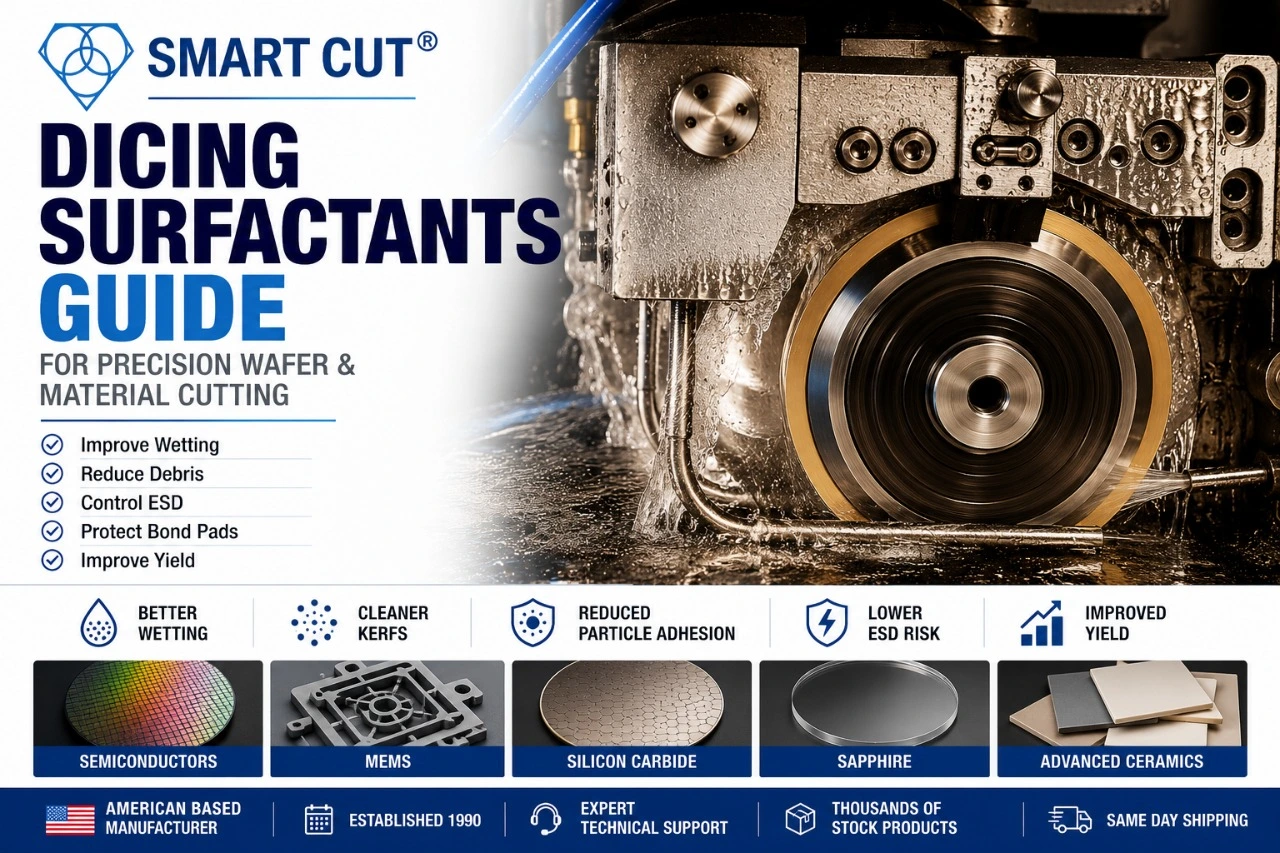
Dicing surfactants support stable and consistent wafer dicing. You use them as part of a complete dicing fluid designed to
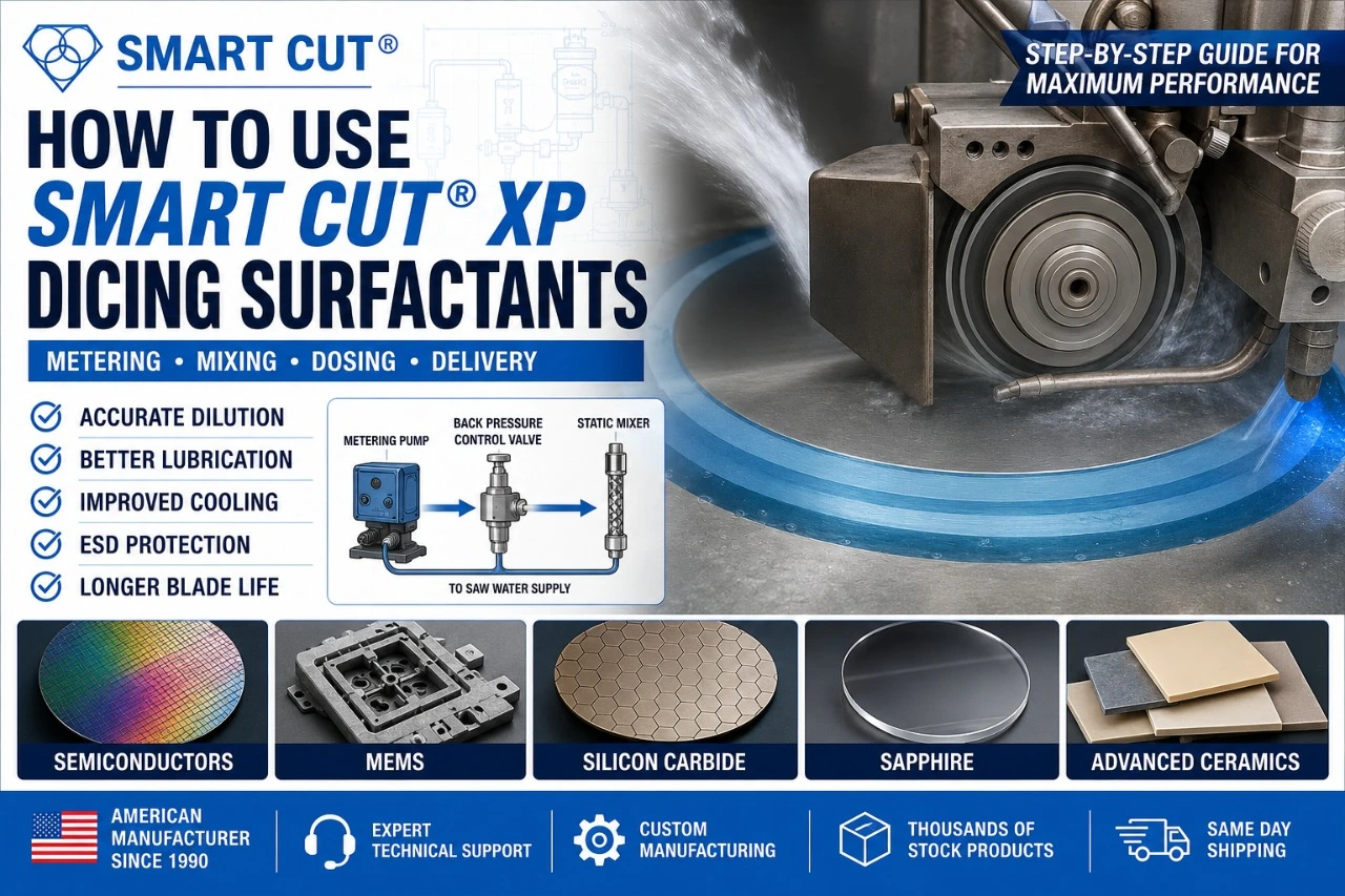
SMART CUT® XP dicing surfactants should be introduced into the saw water supply in a controlled and consistent manner to ensure proper dilution, stable chemical
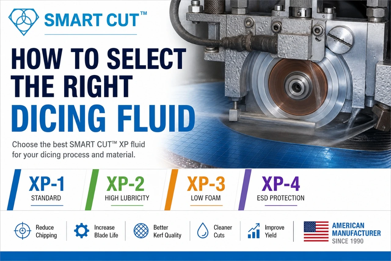
Selecting the correct dicing surfactant / fluid is essential for stable cutting, consistent kerf quality, and long blade life. Each