blog, Cutting

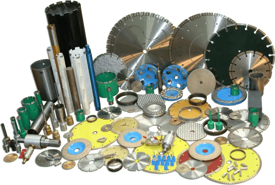
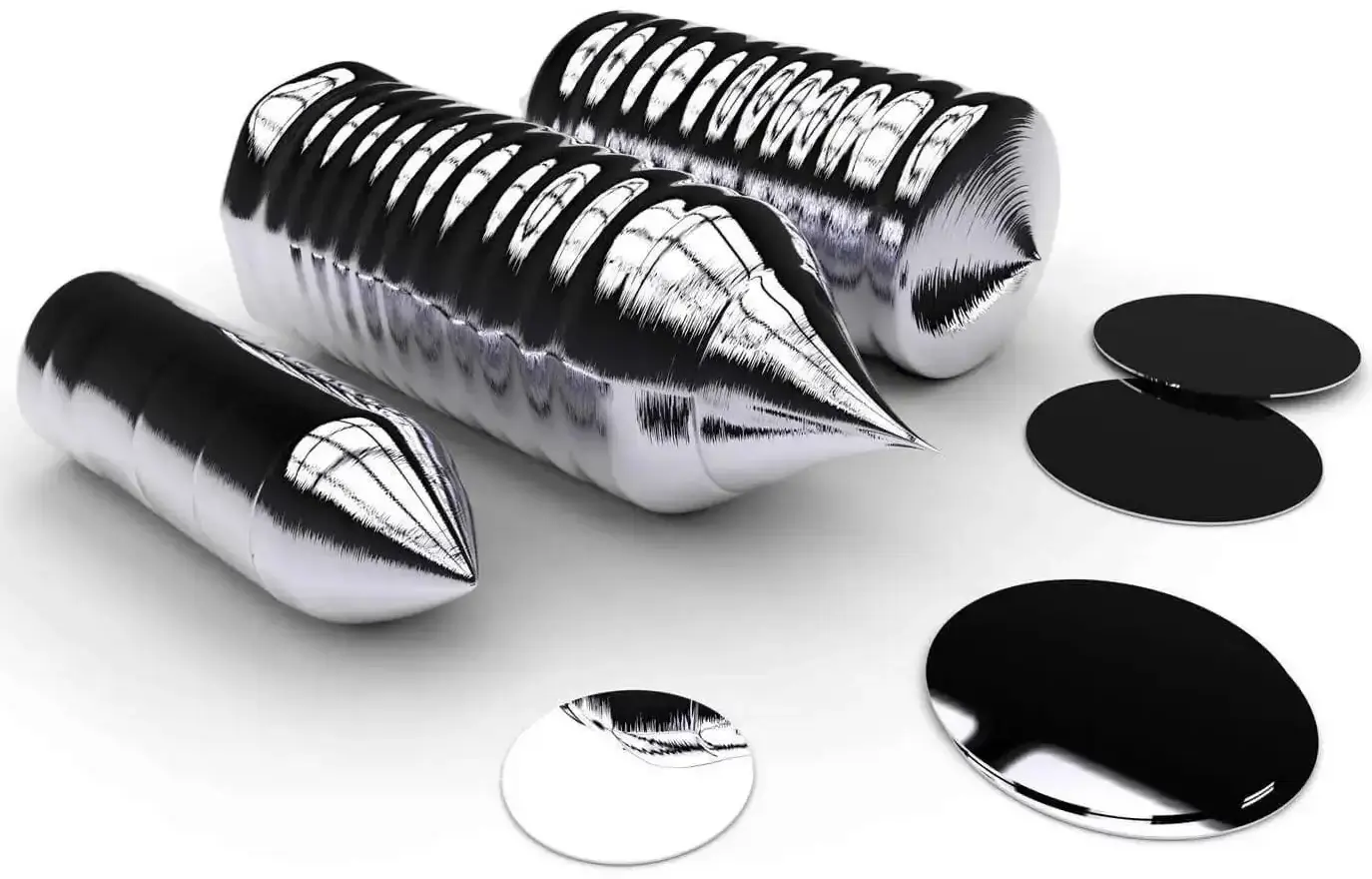
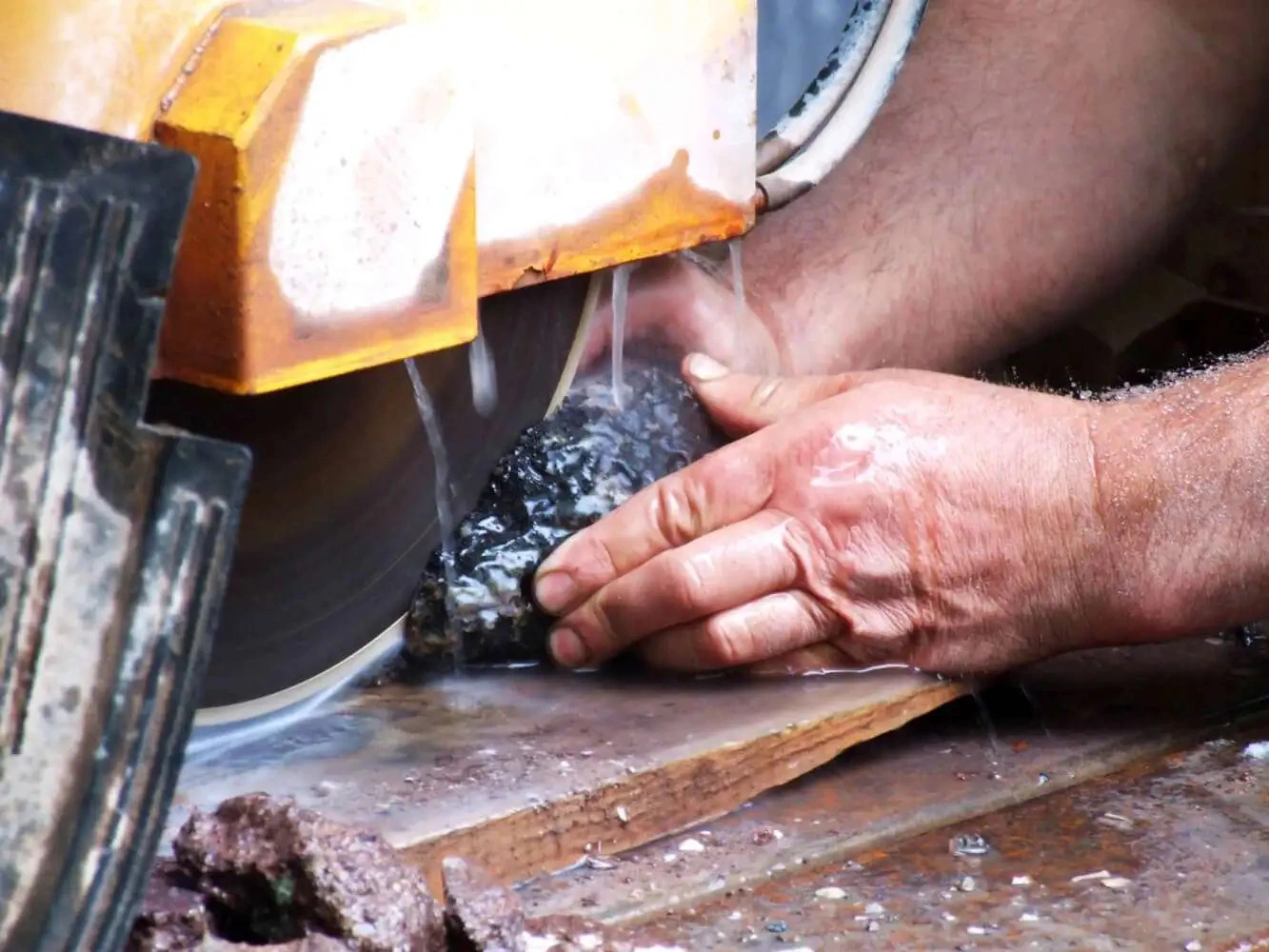
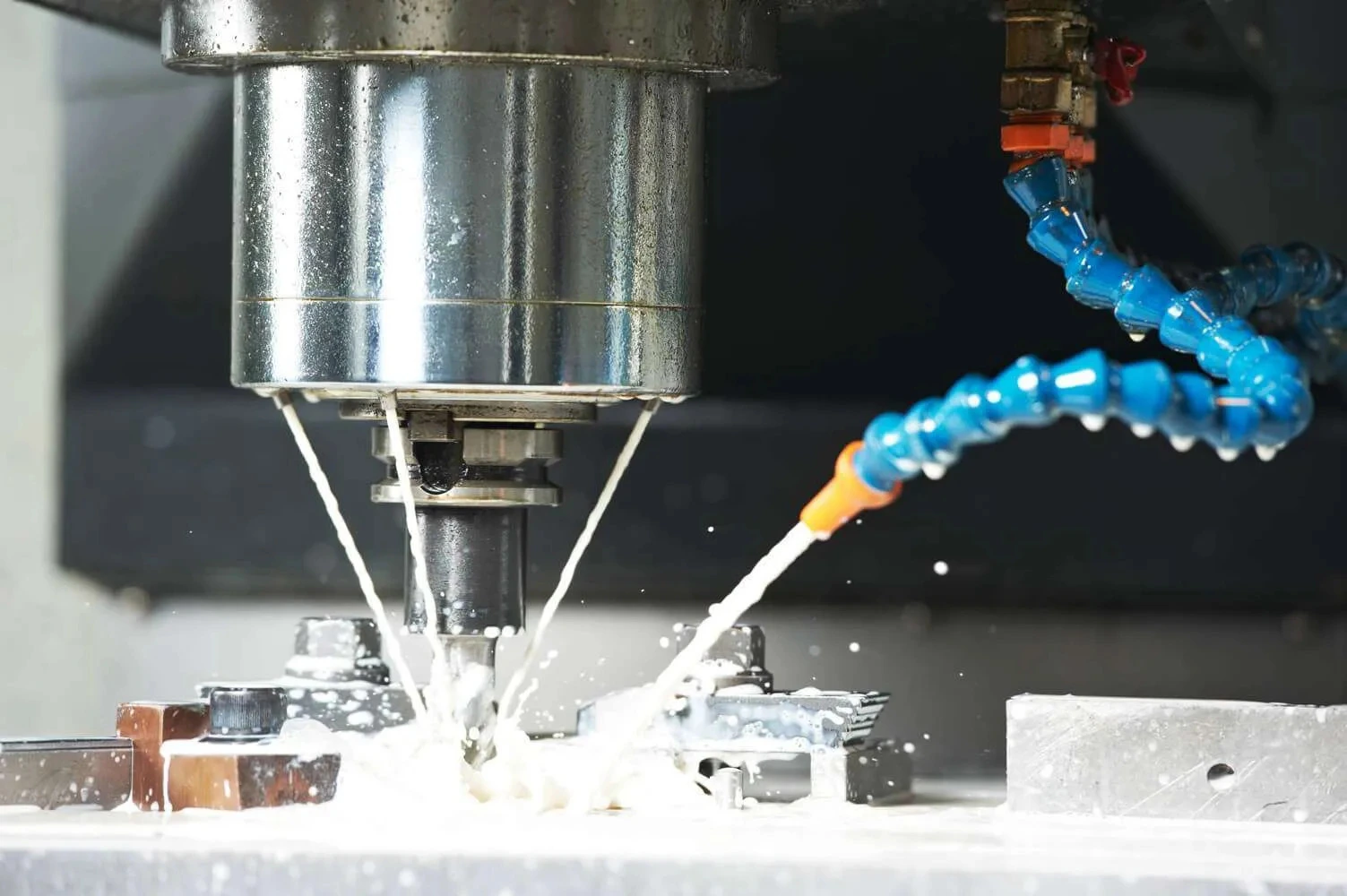
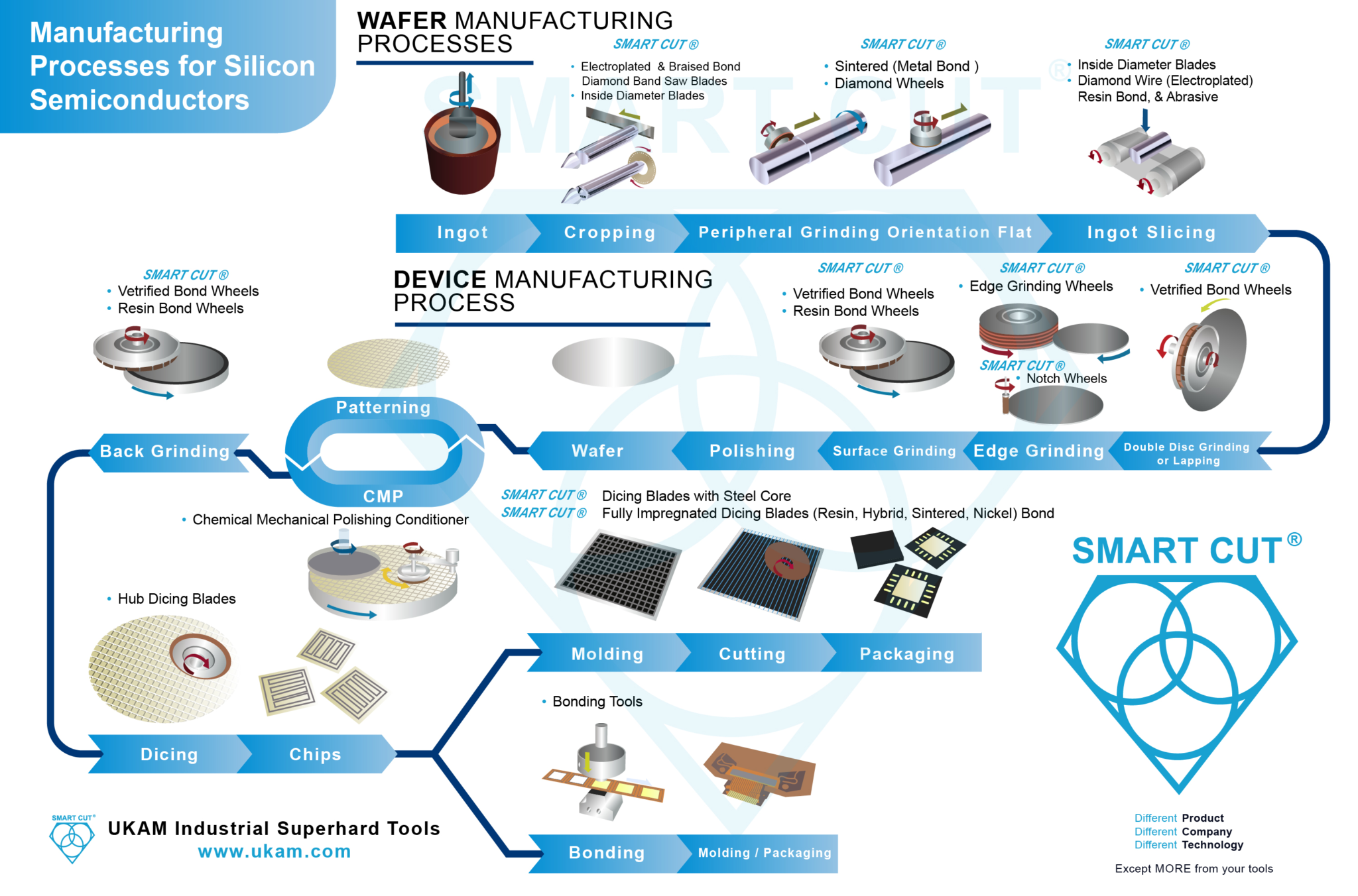
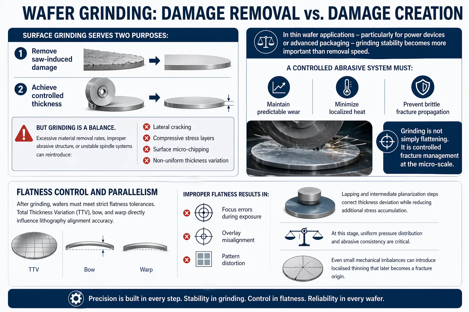
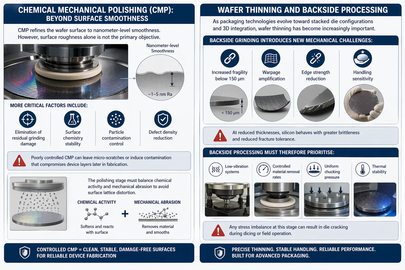
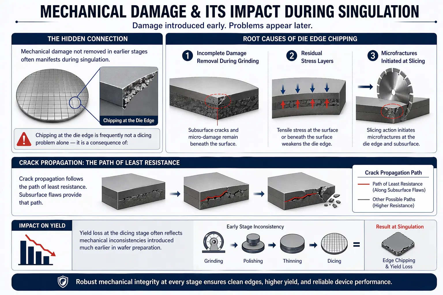
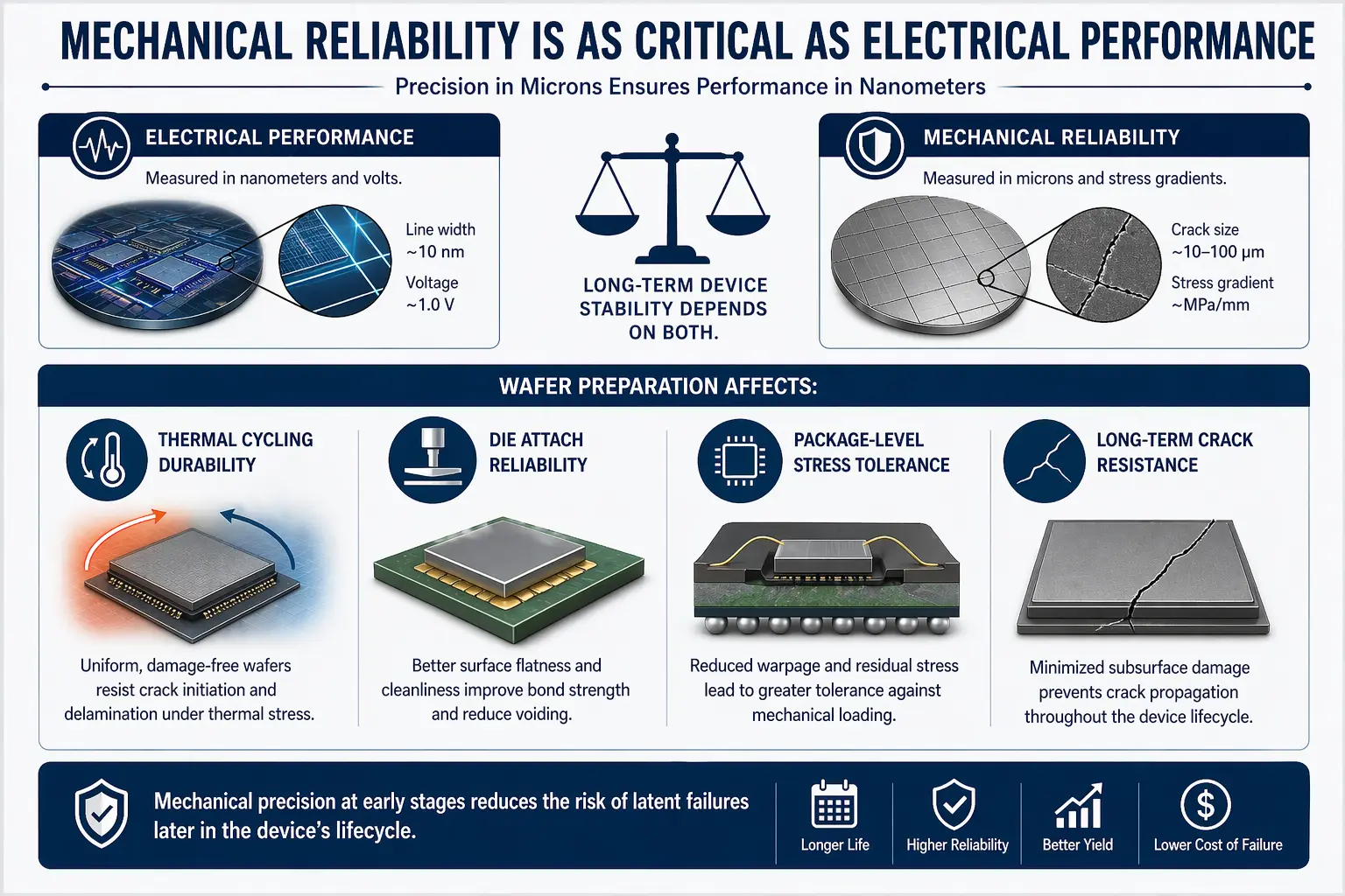
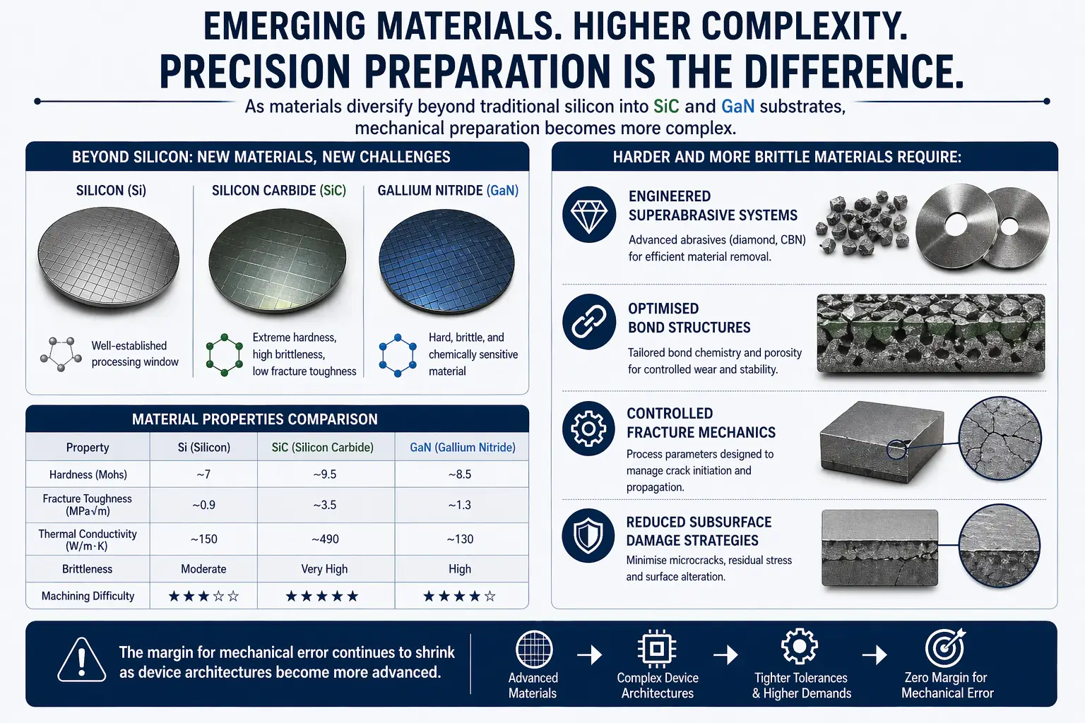
Silicon Wafer Material Preparation: Mechanical Stages That Determine Semiconductor Yield

Silicon Wafer Preparation

Trusted by Tens of Thousands of Manufacturers, Laboratories Research Institutions Worldwide Since 1990

American Based Manufacturer

Established in 1990

Custom manufacturing

Modern semiconductor devices are often discussed in terms of lithography nodes, transistor density, and advanced packaging. However, long before photolithography defines circuit geometry, the mechanical integrity of the silicon wafer has already determined whether high yield is even possible.

Wafer preparation is not simply a preliminary step in semiconductor fabrication. It is the structural foundation that governs flatness stability, fracture resistance, thermal response, and ultimately die reliability.

This article focuses specifically on the mechanical and surface-conditioning stages that influence downstream device performance – without revisiting the broader semiconductor manufacturing flow already covered in our Knowledge Centre.

Crystal Quality Is Only the Starting Point

Single-crystal silicon grown by CZ or Float Zone methods establishes purity and lattice orientation. But crystal perfection at the ingot level does not automatically translate into wafer-level mechanical stability.

During conversion from ingot to wafer, several structural risks are introduced:

● Residual stress from thermal gradients

● Microcrack initiation during slicing

● Surface damage extending below visible roughness

● Edge defects that act as crack propagation sites

The objective of wafer preparation is not only to achieve dimensional targets – it is to remove and control damage introduced during each mechanical stage.

Diamond Wire Slicing and Subsurface Damage Formation

Diamond wire sawing has largely replaced ID saw methods due to efficiency and reduced kerf loss. However, even optimised slicing parameters introduce:

● Amorphous silicon layers

● Microfractures beneath the cut surface

● Surface waviness

● Edge chipping

Subsurface damage depth can extend several microns below the visible surface. If not fully removed during subsequent processing, this damage becomes a latent failure mechanism during thermal cycling or die singulation.
The quality of this initial cut determines how aggressively downstream grinding must operate, which directly affects stress development.

Wafer Grinding: Damage Removal vs. Damage Creation

Surface grinding serves two purposes:

1. Remove saw-induced damage

2. Achieve controlled thickness

But grinding is a balance. Excessive material removal rates, improper abrasive structure, or unstable spindle systems can reintroduce:

● Lateral cracking

● Compressive stress layers

● Surface micro-chipping

● Non-uniform thickness variation

In thin wafer applications – particularly for power devices or advanced packaging – grinding stability becomes more important than removal speed.

A controlled abrasive system must:

● Maintain predictable wear

● Minimize localized heat

● Prevent brittle fracture propagation

Grinding is not simply flattening. It is controlled fracture management at the micro-scale.

Flatness Control and Parallelism

After grinding, wafers must meet strict flatness tolerances. Total Thickness Variation (TTV), bow, and warp directly influence lithography alignment accuracy.

Improper flatness results in:

● Focus errors during exposure

● Overlay misalignment

● Pattern distortion

Lapping and intermediate planarization steps correct thickness deviation while reducing additional stress accumulation.

At this stage, uniform pressure distribution and abrasive consistency are critical. Even small mechanical imbalances can introduce localised thinning that later becomes a fracture origin.

Chemical Mechanical Polishing (CMP) and Surface Integrity

CMP refines the wafer surface to nanometer-level smoothness. However, surface roughness alone is not the primary objective.

More critical factors include:

● Elimination of residual grinding damage

● Surface chemistry stability

● Particle contamination control

● Defect density reduction

Poorly controlled CMP can leave micro-scratches or induce contamination that compromises device layers later in fabrication.

The polishing stage must balance chemical activity and mechanical abrasion to avoid surface lattice distortion.

Wafer Thinning and Backside Processing

As packaging technologies evolve toward stacked die configurations and 3D integration, wafer thinning has become increasingly important.

Backside grinding introduces new mechanical challenges:

● Increased fragility below 150 µm

● Warpage amplification

● Edge strength reduction

● Handling sensitivity

At reduced thicknesses, silicon behaves with greater brittleness and reduced fracture tolerance.

Backside processing must therefore prioritise:

● Low-vibration systems

● Controlled material removal rates

● Uniform chucking pressure

● Thermal stability

Any stress imbalance at this stage can result in die cracking during dicing or field operation.

Dicing Sensitivity and Crack Propagation

Mechanical damage not removed in earlier stages often manifests during singulation.

Chipping at the die edge is frequently not a dicing problem alone — it is a consequence of:

● Incomplete damage removal during grinding

● Residual stress layers

● Microfractures initiated at slicing

Crack propagation follows the path of least resistance. Subsurface flaws provide that path.

Yield loss at the dicing stage often reflects mechanical inconsistencies introduced much earlier in wafer preparation.

Why Mechanical Preparation Directly Impacts Device Reliability

Electrical performance is often measured in nanometers and volts. Mechanical reliability is measured in microns and stress gradients.

However, long-term device stability depends on both.

Wafer preparation affects:

● Thermal cycling durability

● Die attach reliability

● Package-level stress tolerance

● Long-term crack resistance

Mechanical precision at early stages reduces the risk of latent failures later in the device’s lifecycle.

Emerging Challenges in Advanced Substrates

As materials diversify beyond traditional silicon into SiC and GaN substrates, mechanical preparation becomes more complex.

Harder and more brittle materials require:

● Engineered superabrasive systems

● Optimised bond structures

● Controlled fracture mechanics

● Reduced subsurface damage strategies

The margin for mechanical error continues to shrink as device architectures become more advanced.

Short FAQs

Depending on parameters, damage can extend several microns beneath the visible surface and must be removed during grinding.

Reduced thickness lowers fracture resistance and increases sensitivity to stress concentration.

Yes. Mechanical material removal remains essential for maintaining thickness control and preventing damage.

Often, it originates from microfractures introduced during earlier slicing or grinding stages.

Trusted by Tens of Thousands of Manufacturers, Laboratories,
Research Institutions Worldwide Since 1990

American Based Manufacturer

Established in 1990

Custom manufacturing

Brian is an experienced professional in the field of precision cutting tools, with over 27 years of experience in technical support. Over the years, he has helped engineers, manufacturers, researchers, and contractors find the right solutions for working with advanced and hard-to-cut materials. He’s passionate about bridging technical knowledge with real-world applications to improve efficiency and accuracy.

As an author, Brian Farberov writes extensively on diamond tool design, application engineering, return on investment strategies, and process optimization, combining technical depth with a strong understanding of customer needs and market dynamics.

author-avatar

About Brian Farberov

Brian is an experienced professional in the field of precision cutting tools, with over 27 years of experience in technical support. Over the years, he has helped engineers, manufacturers, researchers, and contractors find the right solutions for working with advanced and hard-to-cut materials. He’s passionate about bridging technical knowledge with real-world applications to improve efficiency and accuracy. As an author, Brian Farberov writes extensively on diamond tool design, application engineering, return on investment strategies, and process optimization, combining technical depth with a strong understanding of customer needs and market dynamics.