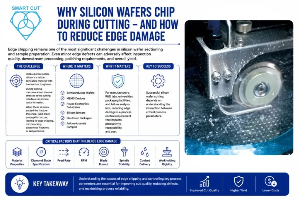











Why Silicon Wafers Chip During Cutting – And How to Reduce Edge Damage
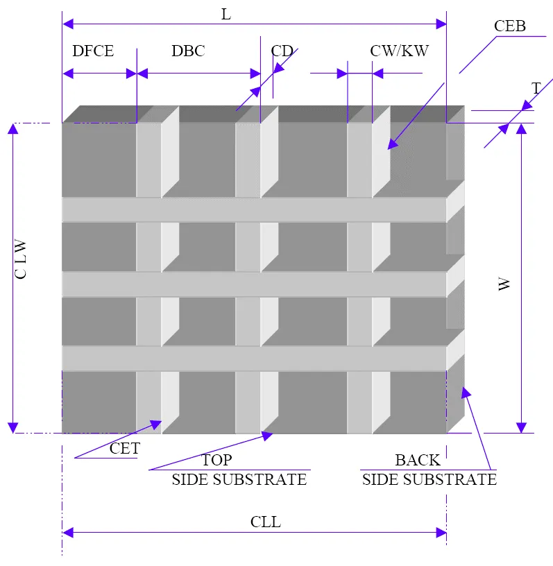
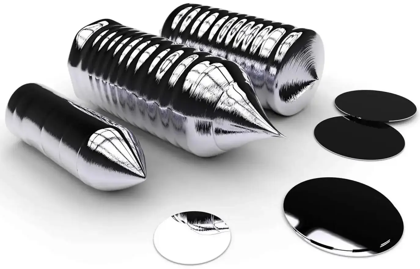
Edge chipping remains one of the most significant challenges in silicon wafer sectioning and sample preparation. Whether cutting semiconductor wafers, MEMS devices, power electronics substrates, silicon sensors, electronic packages, or failure-analysis samples, even minor edge defects can adversely affect inspection quality, downstream processing, polishing requirements, and overall yield.
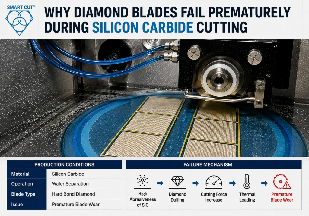
Why Diamond Blades Fail Prematurely During Silicon Carbide Cutting
A manufacturer producing silicon carbide substrates for power electronics and semiconductor applications experienced severe diamond blade wear during precision slotting and wafer separation operations. Blade life dropped below acceptable production thresholds within weeks after transitioning from alumina-based ceramic components to silicon carbide. Operators reported increasing spindle load, thermal discoloration near cut edges, unstable kerf width, and excessive dressing frequency during long production runs.
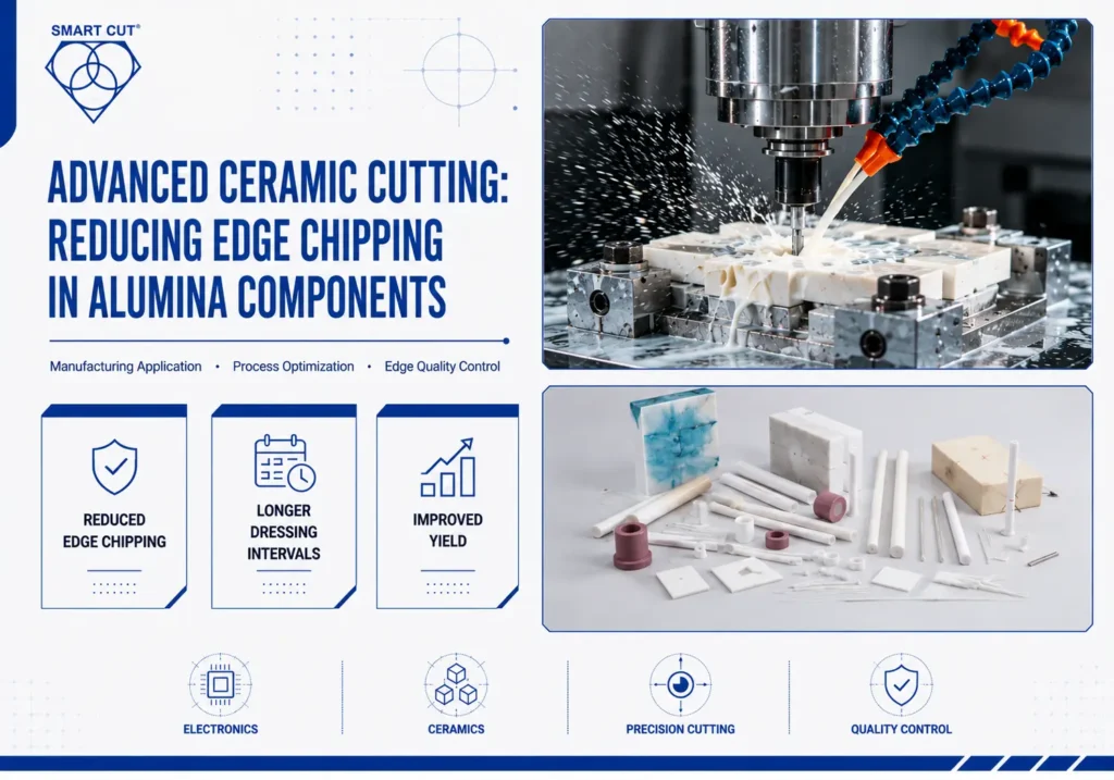
Advanced Ceramic Cutting: Reducing Edge Chipping in Alumina Components
Edge chipping remains one of the most common and costly challenges when machining advanced ceramic materials. While dimensional tolerances may remain within specification, microscopic edge damage can propagate during downstream processing, resulting in scrap, rework, assembly failures, and reduced component reliability.
Cutting Glass with Diamond Saw Blades: How to Prevent Chipping, Cracking & Material Loss
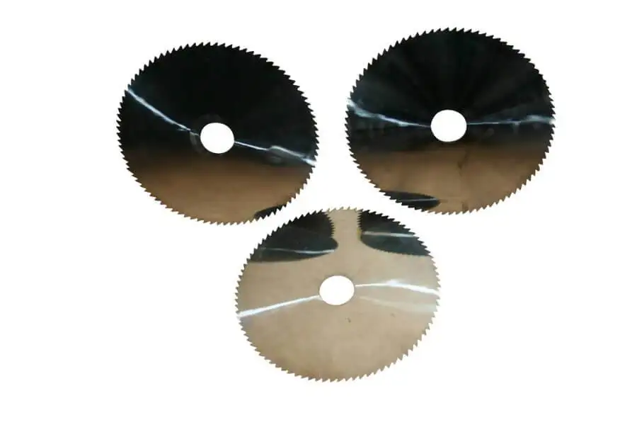
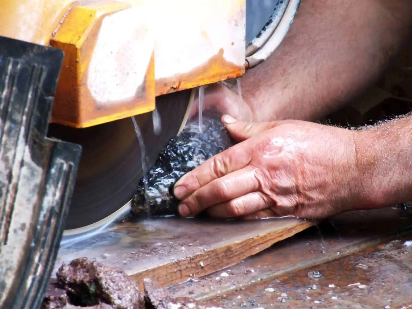
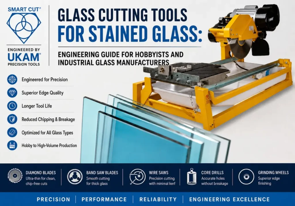
Edge chipping, corner breakout, microcracking, poor surface finish, and excessive material loss are among the most common challenges encountered when cutting glass. While separating the material may appear straightforward, producing clean, damage-free cuts consistently is often one of the most difficult steps in the manufacturing process.
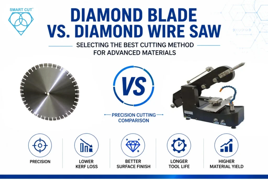
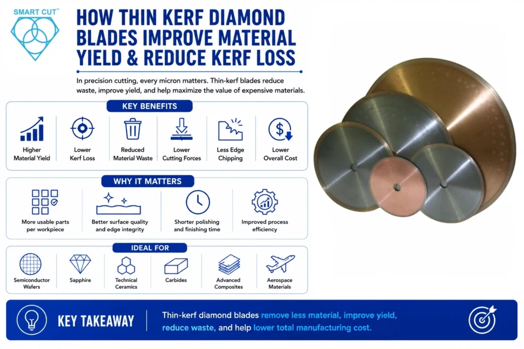
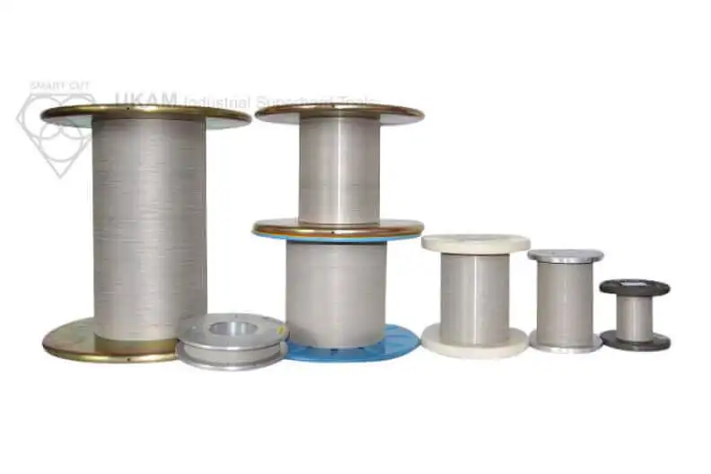
Diamond Wire Saw: Maximizing Material Yield and Precision Cutting of Advanced Materials
Manufacturers processing sapphire, germanium, silicon, quartz, technical ceramics, optical crystals, and advanced electronic materials face a common challenge: every cut removes material, introduces some degree of stress, and influences the quality of every downstream operation.
How Laboratory Cutting Machines Improve Precision Sectioning
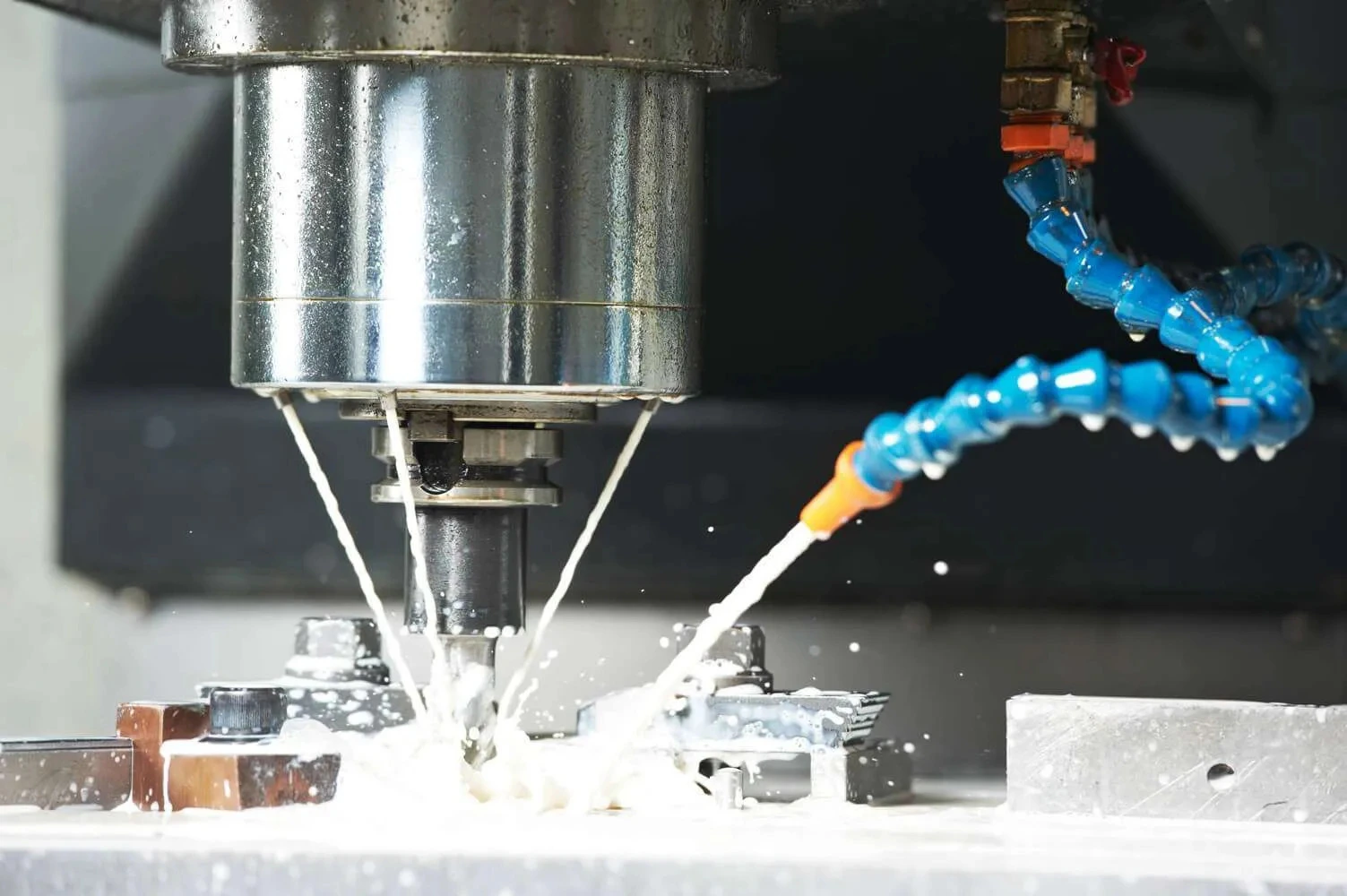
In precision material preparation, the quality of the cut directly affects inspection accuracy, edge integrity, dimensional reliability, polishing time, and downstream analytical results. Standard abrasive cutting equipment often introduces excessive heat, vibration, edge chipping, microcracks, subsurface fractures, coating separation, or material deformation — particularly when sectioning brittle, ultra-hard, composite, or advanced engineering materials.
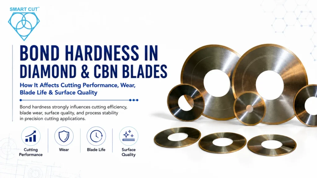
Critical Factors That Influence Diamond Dicing Blade Cutting Performance
Diamond dicing blades are essential tools for high-precision cutting in semiconductor manufacturing, electronics packaging, advanced ceramics, and optical materials. These blades enable manufacturers to separate delicate substrates with extremely tight tolerances while minimizing material damage.
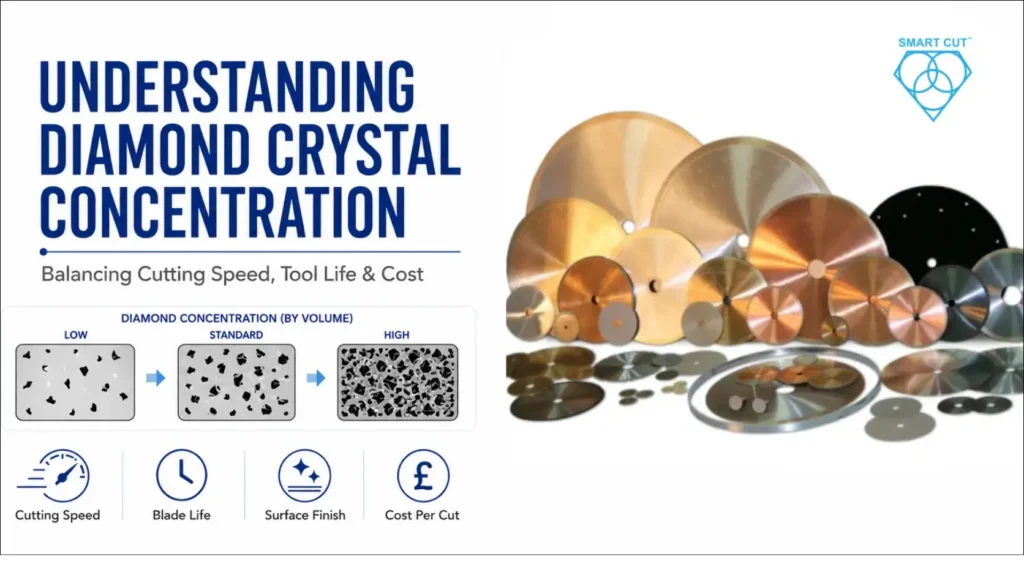
How Diamond Grit Size Influences Cutting Speed, Surface Finish, and Tool Life
Diamond grit size is one of the most significant factors influencing the performance of diamond debt cutting, grinding, and polishing tools. While operators in many applications may focus on machine settings, feed rates, or coolant conditions, they often ignore the fact that, like any material, diamond abrasive particle size is a fundamental requirement that dictates tool/material interaction.
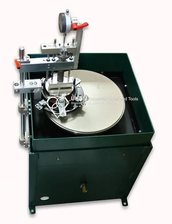
Silicon Wafer Material Preparation: Mechanical Stages That Determine Semiconductor Yield
Modern semiconductor devices are often discussed in terms of lithography nodes, transistor density, and advanced packaging. However, long before photolithography defines circuit geometry, the mechanical integrity of the silicon wafer has already determined whether high yield is even possible.