


01
Jun
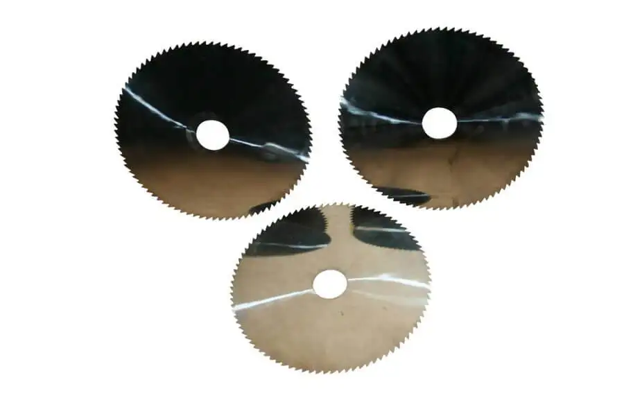
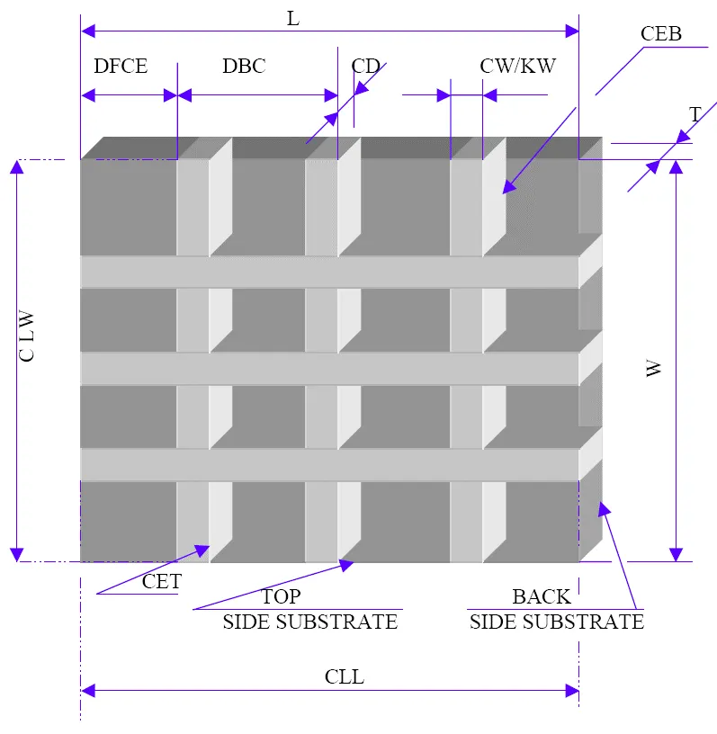
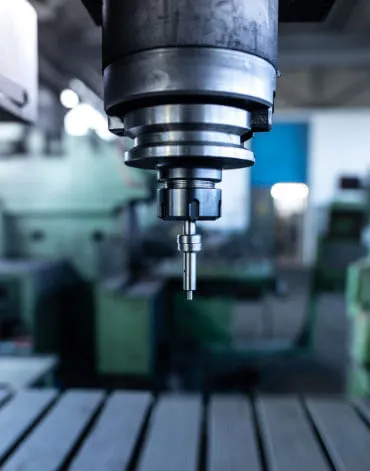
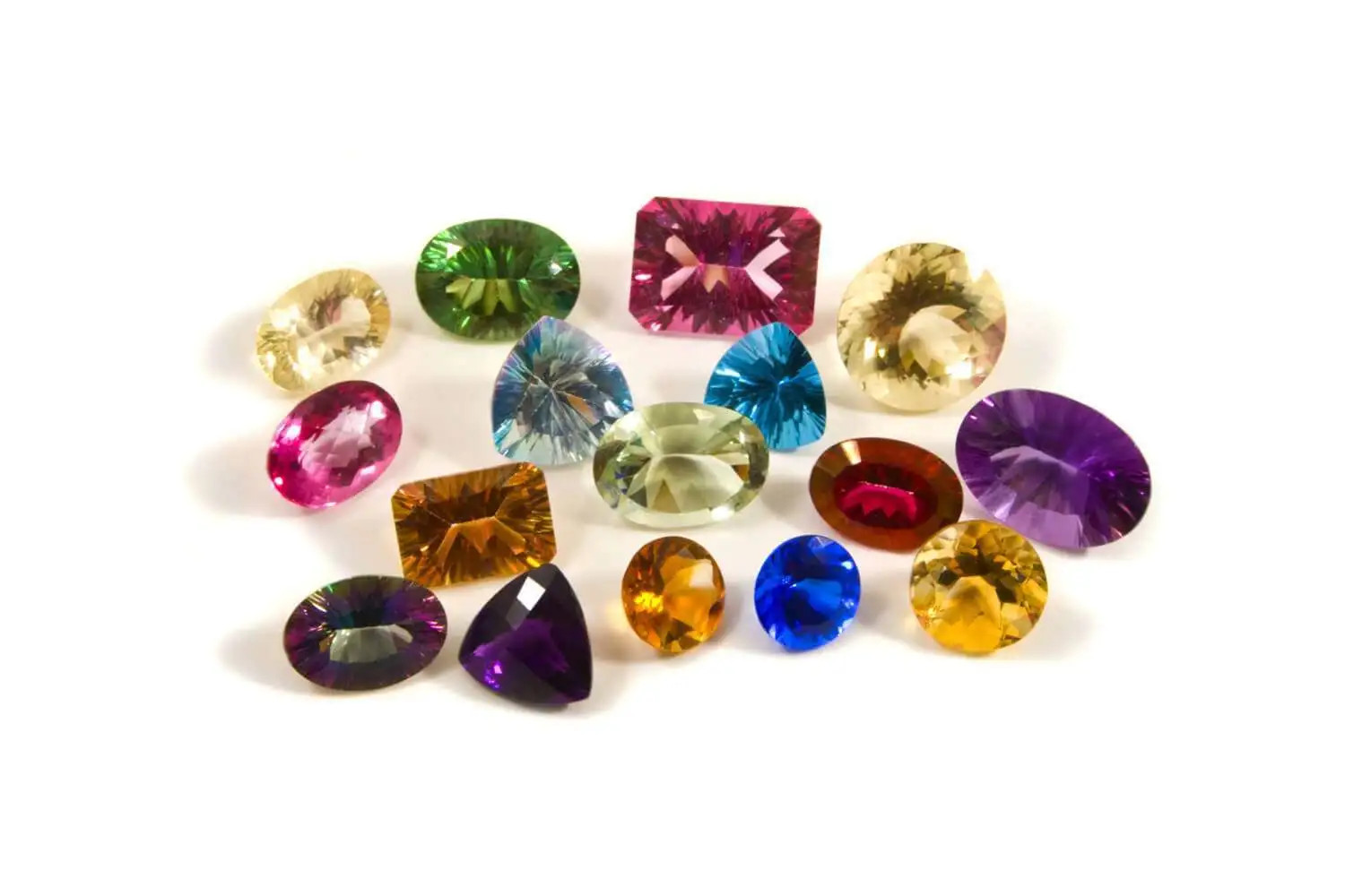
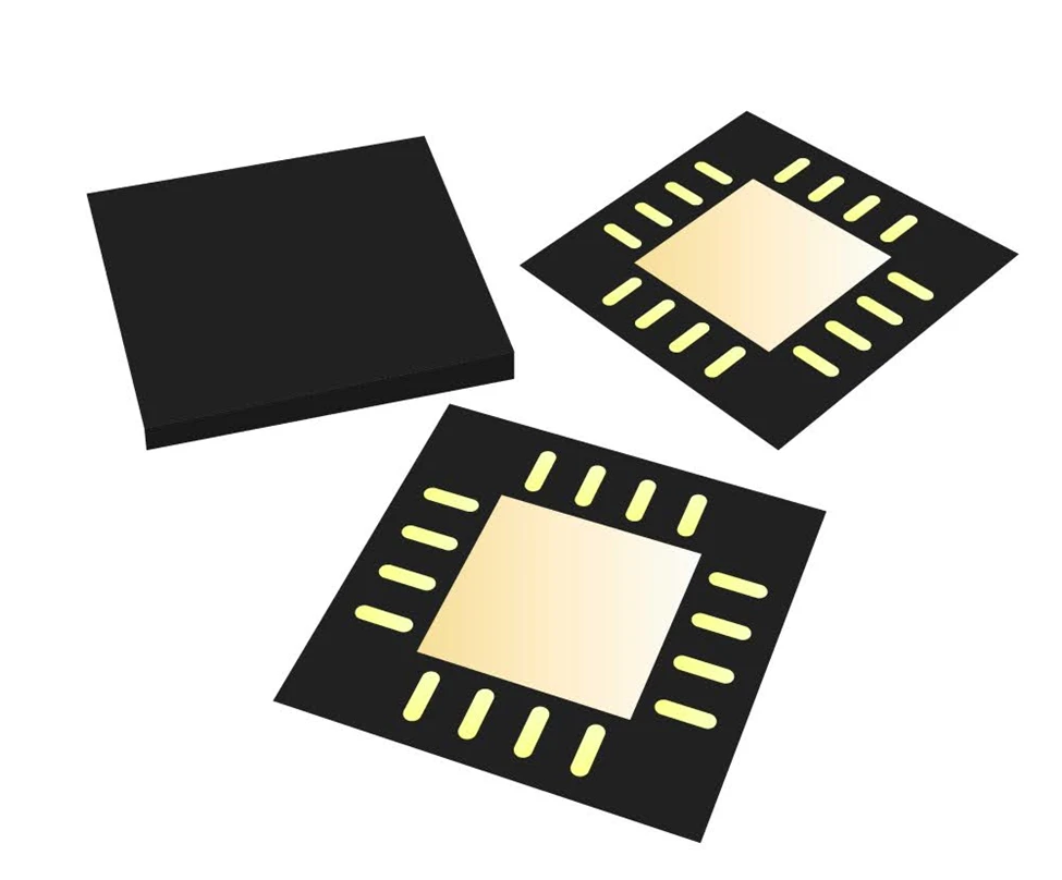
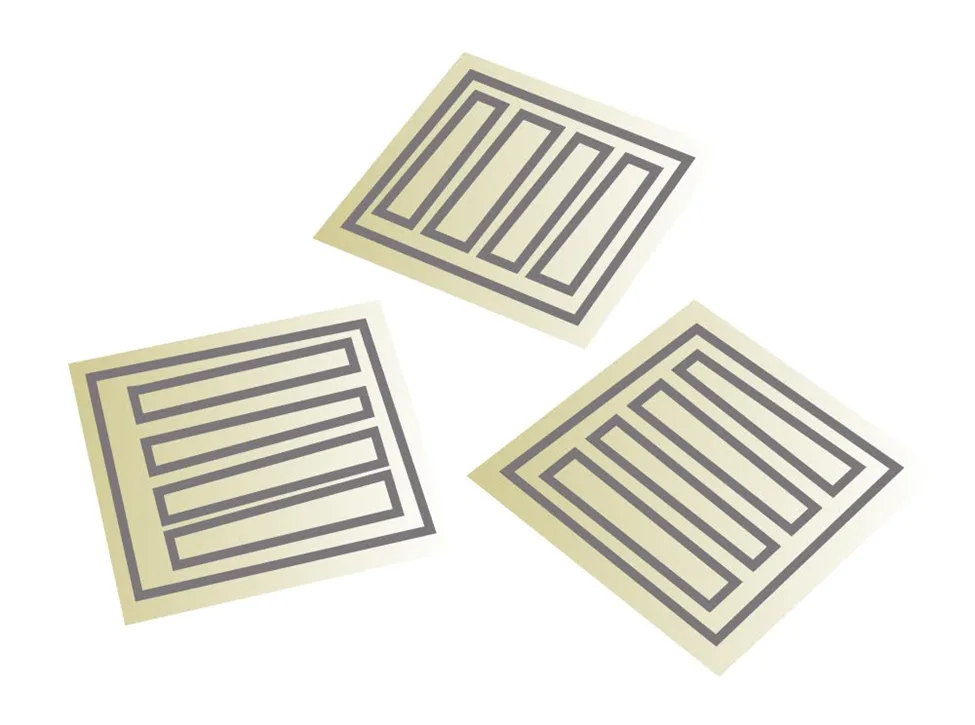
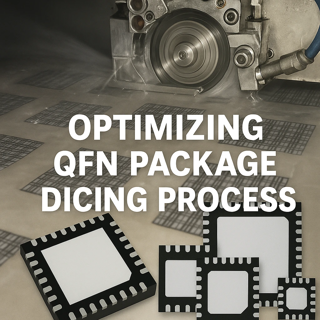
Optimizing QFN Package Dicing Process Using SMART CUT® Dicing Blades
Trusted by Tens of Thousands of Manufacturers, Laboratories,
Research Institutions Worldwide
Since 1990
American Based Manufacturer
Established in 1990
Expert technical support
Custom manufacturing
Thousands of Stock Products
Same day shipping
Share this Article with Friend or Colleague
Dicing QFN packages presents...

01
Jun
Select right Diamond Dicing Blade for your application
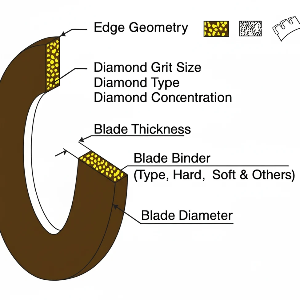
Selecting the right dicing blade for your application requires careful consideration of several key variables that influence both performance and cost. The type of material being cut, the depth of the required cuts, the level...
02
Jun
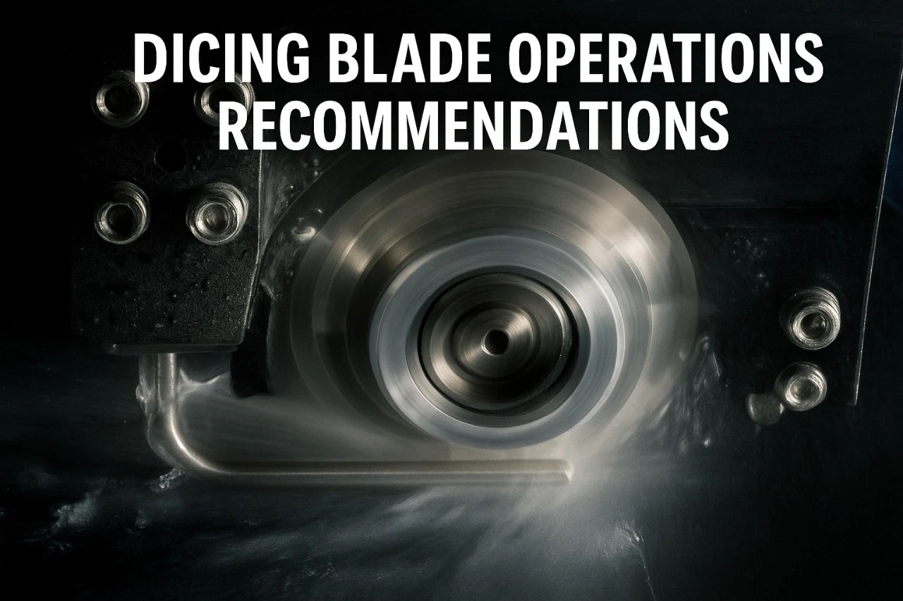
Dicing Blade Operations Recommendations
Trusted by Tens of Thousands of Manufacturers, Laboratories,
Research Institutions Worldwide
Since 1990
American Based Manufacturer
Established in 1990
Expert technical support
Custom manufacturing
Thousands of Stock Products
Same day shipping
Share this Article with Friend or Colleague
Selecting the right dicing...
02
Jun
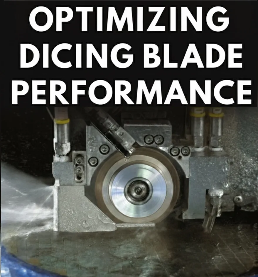
Optimizing your Diamond Dicing Performance
Trusted by Tens of Thousands of Manufacturers, Laboratories,
Research Institutions Worldwide
Since 1990
American Based Manufacturer
Established in 1990
Expert technical support
Custom manufacturing
Thousands of Stock Products
Same day shipping
Share this Article with Friend or Colleague
The performance of diamond...
02
Jun
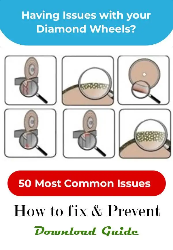
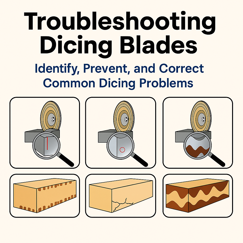
Trouble Shooting Dicing Problems
Guide on most common dicing problems and how to resolve themShare this Article with Friend or Colleague
ARE YOU USING RIGHT TOOLS
FOR YOUR APPLICATION?
LET USHELP YOU
CONTACT US
HAVING ISSUES WITH
YOUR...
02
Jun
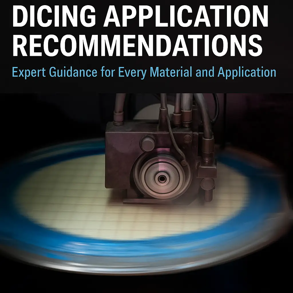
Application Recommendations
Trusted by Tens of Thousands of Manufacturers, Laboratories,
Research Institutions Worldwide
Since 1990
American Based Manufacturer
Established in 1990
Expert technical support
Custom manufacturing
Thousands of Stock Products
Same day shipping
This article provides important guidelines for optimizing the dicing process in...
02
Jun
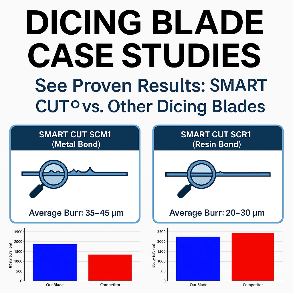
Dicing Blade Case Studies
Trusted by Tens of Thousands of Manufacturers, Laboratories,
Research Institutions Worldwide
Since 1990
American Based Manufacturer
Established in 1990
Expert technical support
Custom manufacturing
Thousands of Stock Products
Same day shipping
Selecting the right dicing blade is important to achieving high yields,...
27
Aug
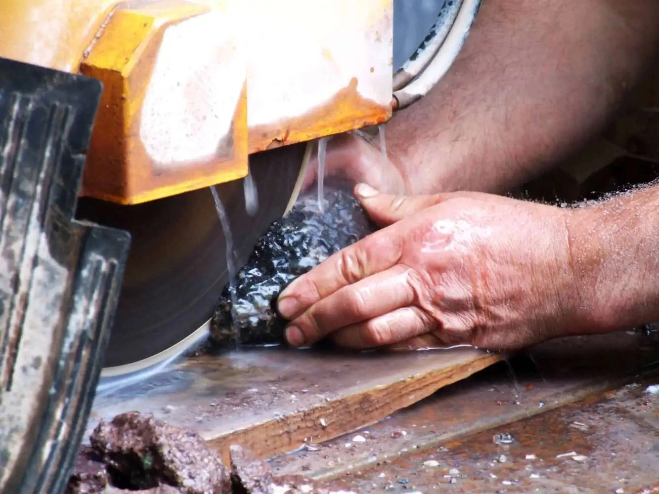
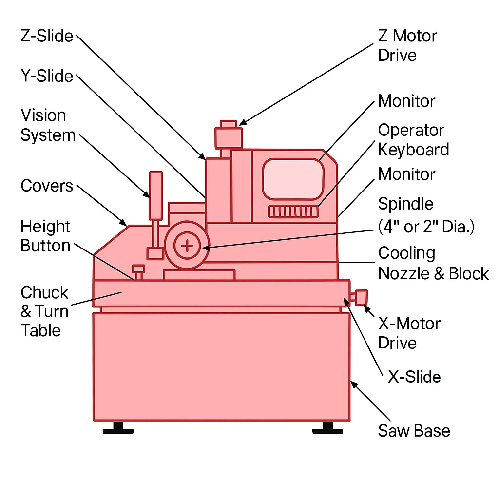
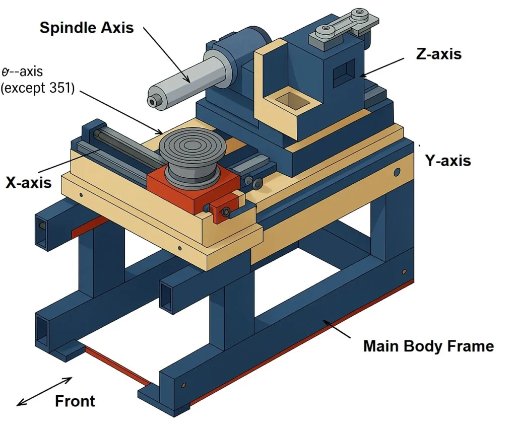
Selecting the Right Wafer Dicing Saw Practical Guide
Selecting the proper wafer dicing saw is a important decision for manufacturers, researchers, and engineers working with large variety of materials. Whether processing silicon wafers in microelectronics, ceramics in materials science, or glass substrates in...

17
Sep
Total Cost of Ownership – Measuring the Real Economics of Diamond Dicing
Many companies still judge diamond dicing blades by purchase price alone. At first, the cheapest blade may appear to be the best choice. However, price does not equal cost. The real economics of diamond dicing...
18
Sep
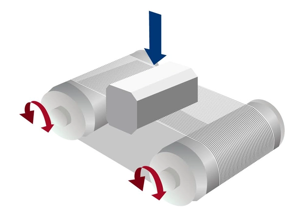
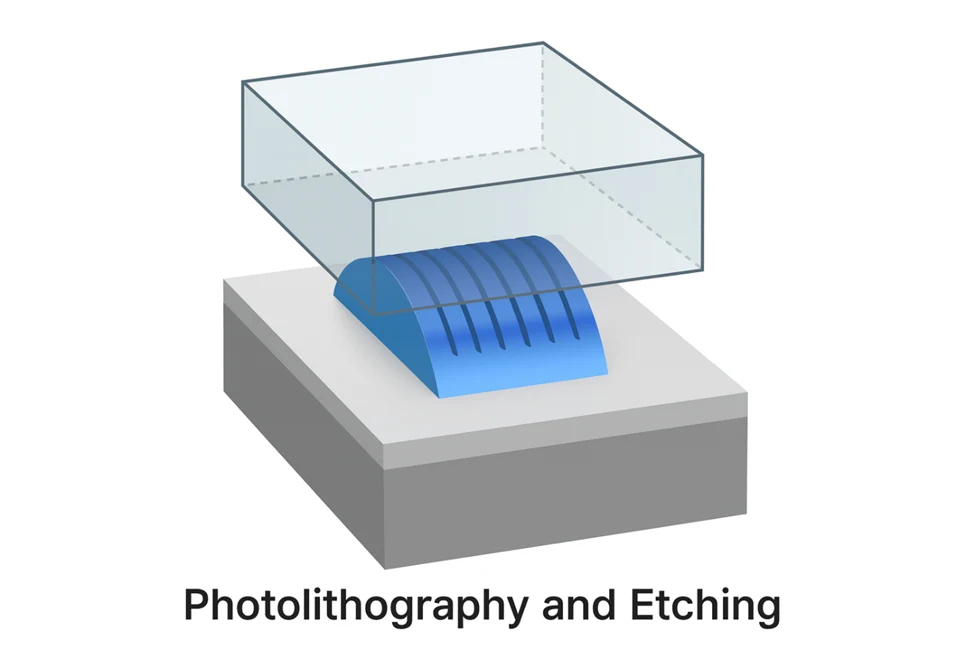
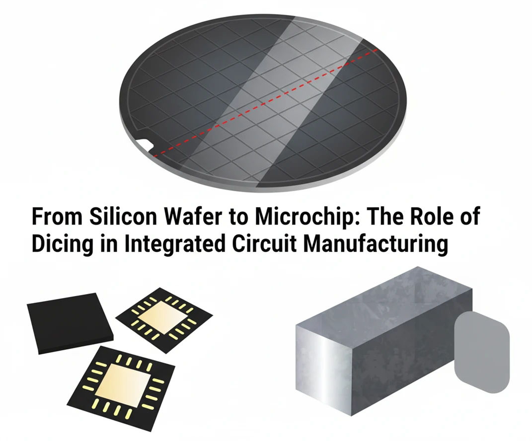
From Silicon Wafer to Microchip: The Role of Dicing in Integrated Circuit Manufacturing
The making of the integrated circuit is a long and complex process that involves many critical steps. In most cases, the wafer travels to multiple facilities before it is completed and turned into the final...
19
Sep
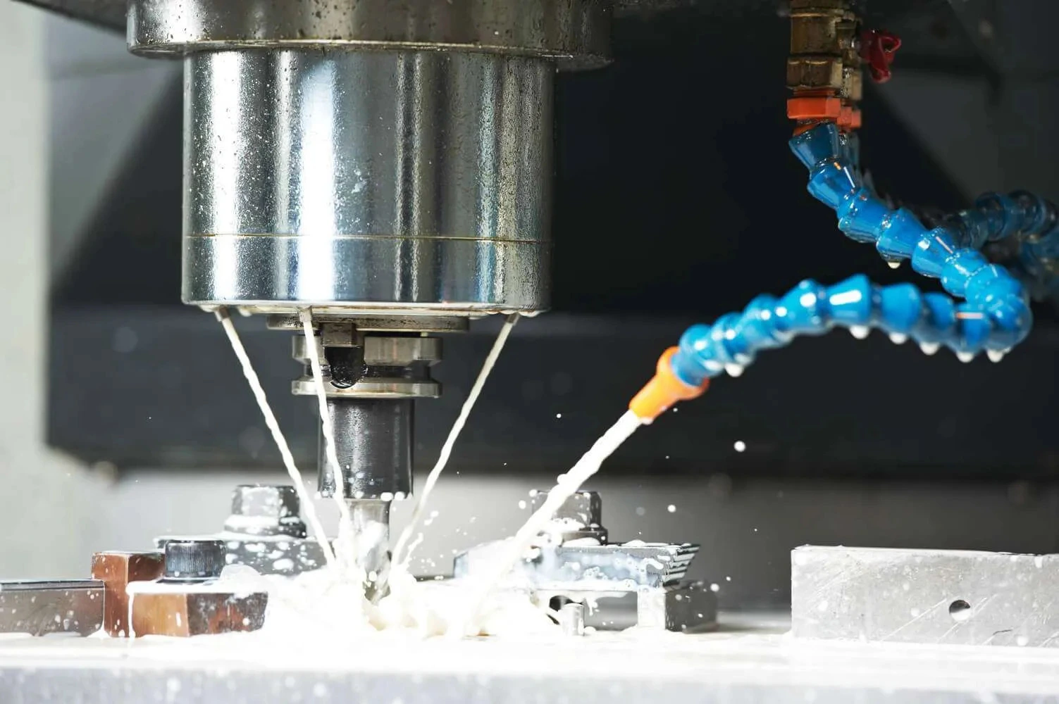
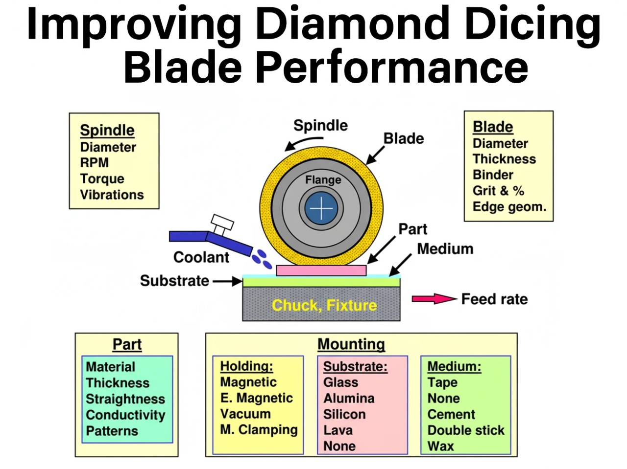
Improving Diamond Dicing Blade Performance: Key Factors and Strategies
Diamond dicing is one of the most important step in semiconductor & microelectronics manufacturing package. Although the process itself does not add direct value to the finished device, it has a decisive impact on yield,...
26
Nov
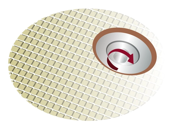
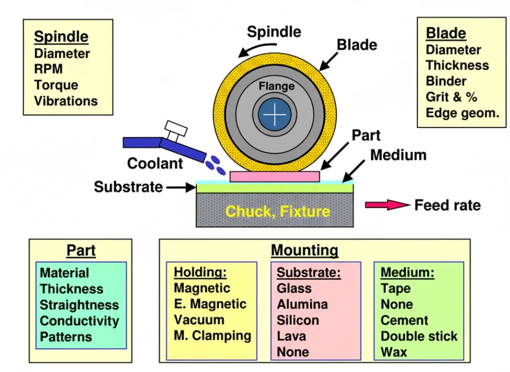
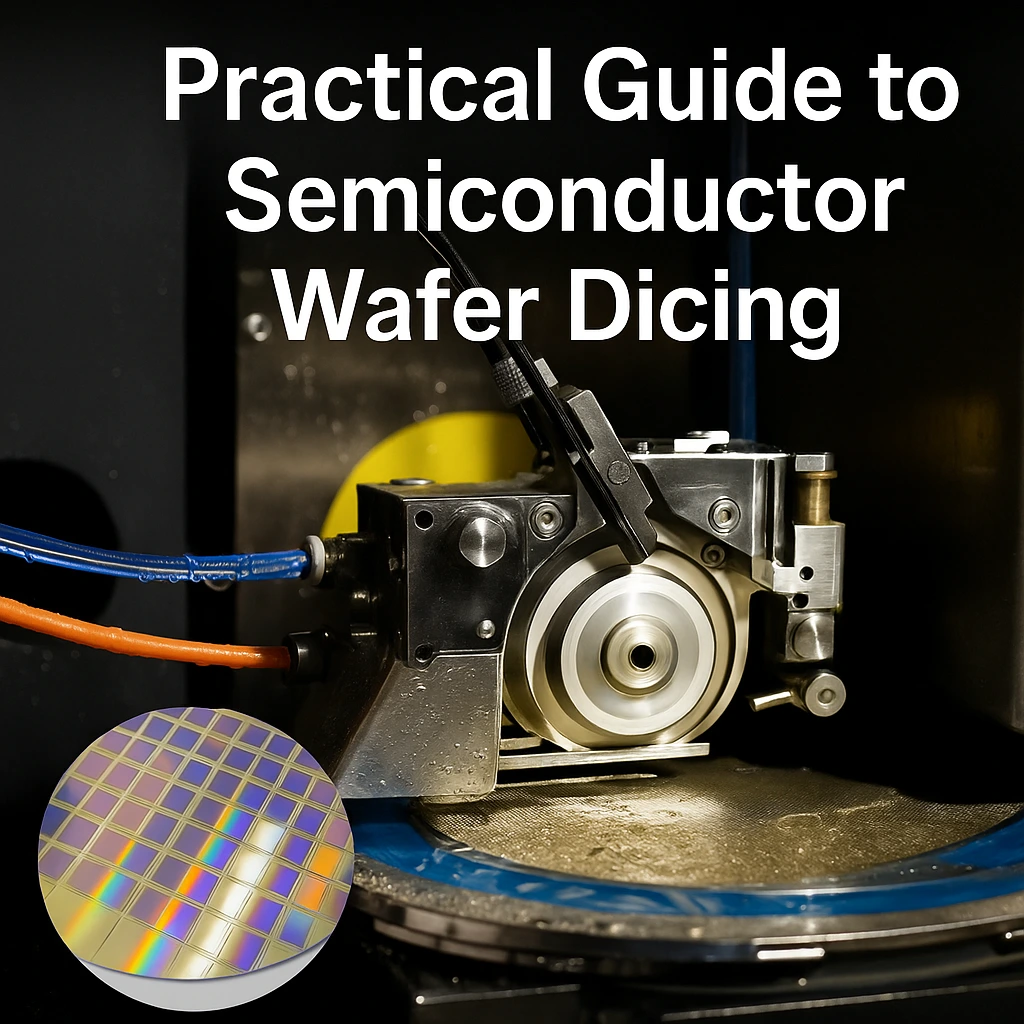
Practical Guide to Semiconductor Wafer Dicing: Materials, Blades, and Process Optimization
Semiconductor wafers are the foundation of nearly all modern electronics, from integrated circuits and photonic devices to advanced power components. As device geometries shrink and packaging density increases, the requirements placed on wafer dicing processes...
08
Dec
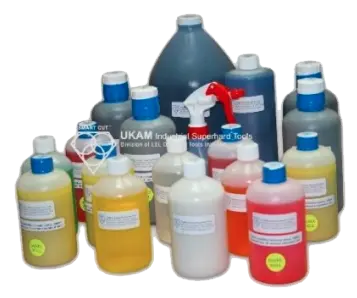
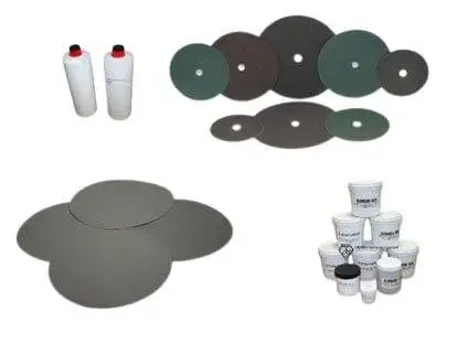
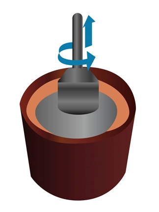
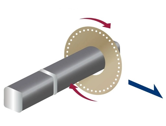
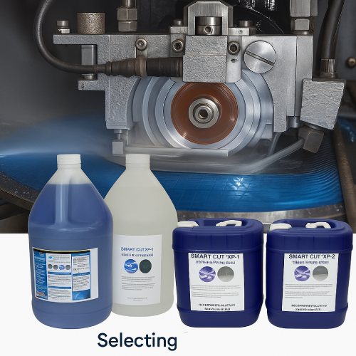
Selecting the Right Dicing Surfactant / Fluid for Your Application
Selecting the correct dicing surfactant / fluid is essential for stable cutting, consistent kerf quality, and long blade life. Each operation places specific demands on lubrication, cooling, foaming control, and electrostatic behavior. You must choose...
09
Dec
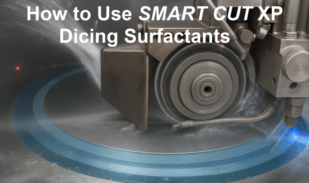
How to Use SMART CUT XP Dicing Surfactants
SMART CUT® XP dicing surfactants should be introduced into the saw water supply in a controlled and consistent manner to ensure proper dilution, stable chemical performance, and uniform delivery to the cutting zone. Correct dosing equipment and proper setup help achieve full...
09
Dec
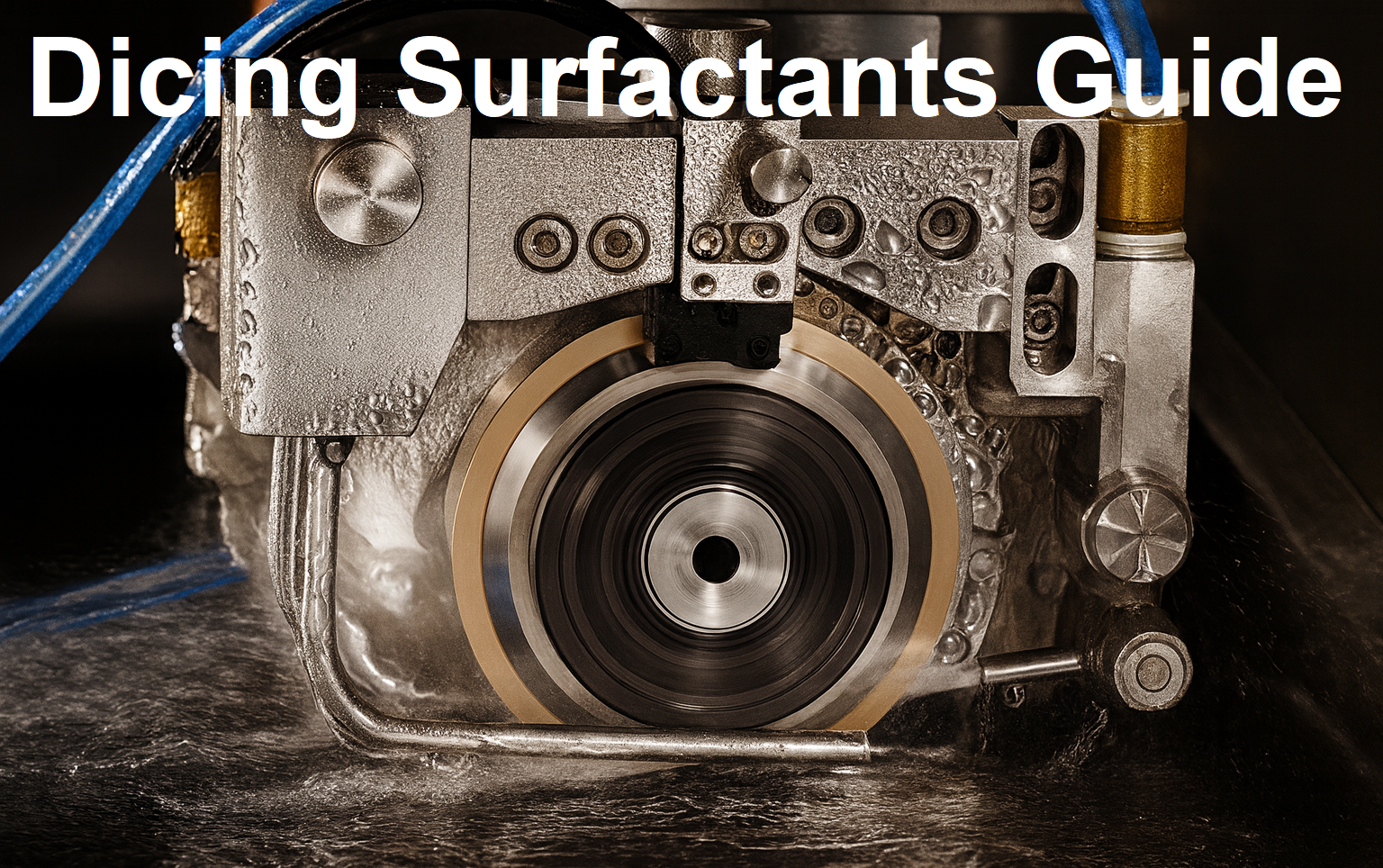
Dicing Surfactants Guide
Dicing surfactants support stable and consistent wafer dicing. You use them as part of a complete dicing fluid designed to cool the blade, flush debris, and protect exposed device surfaces. Modern semiconductor wafers contain smaller...