


Practical Guide to Semiconductor Wafer Dicing: Materials, Blades, and Process Optimization
02
Sep


01
Jun
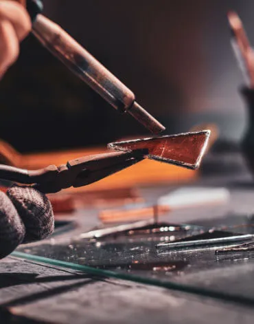
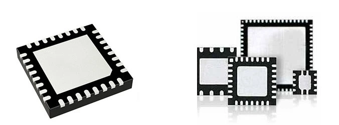
Optimizing QFN Package Dicing Process Using SMART CUT® Dicing Blades
Share this Article with Friend or Colleague
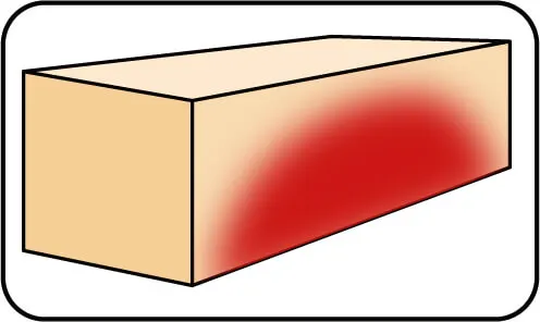
Dicing QFN packages presents several challenges due to the composition of materials and the precision required for clean, defect-free cuts. These challenges arise from the multi-layered structure of...

01
Jun
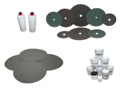
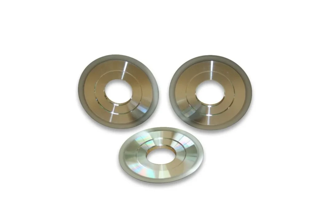
Select right Diamond Dicing Blade for your application
Share this Article with Friend or Colleague
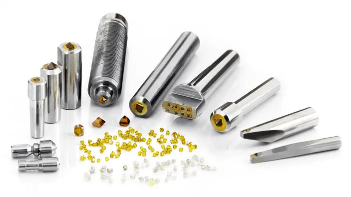
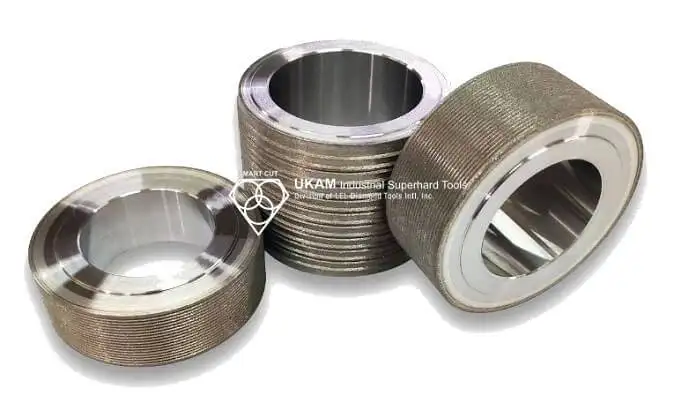
Selecting the right dicing blade for your application requires careful consideration of several key variables that influence both performance and cost. The type of material being cut, the...

02
Jun
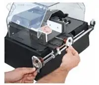
Dicing Blade Operations Recommendations
Share this Article with Friend or Colleague
Selecting the right dicing blade parameters often involves a trial and error process, many aspects of which can be mitigated through experience and a deep understanding of how...

02
Jun
Optimizing Dicing Blade Performance
There are many variables that affect dicing blade performance. Each variable of the dicing process is only of the many components of a larger dicing system (equation). Changing one component or variable of...

02
Jun
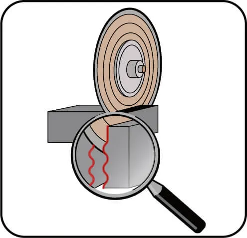
Trouble Shooting Dicing Problems
Guide on most common dicing problems and how to resolve them
Share this Article with Friend or Colleague
ARE YOU USING RIGHT TOOLS
FOR YOUR APPLICATION?
LET USHELP YOU
CONTACT US
HAVING ISSUES WITH
YOUR CURRENT TOOLS?
What...

02
Jun
Application Recommendations
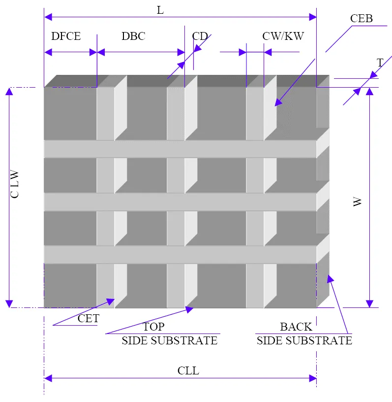
This article provides important guidelines for optimizing the dicing process in semiconductor packaging, focusing on package singulation for various technologies such as BGA, QFN, LED, CMOS, and wafer substrates. It covers key variables such as...

02
Jun
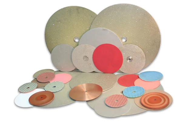
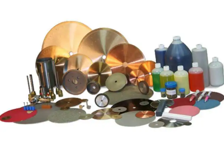
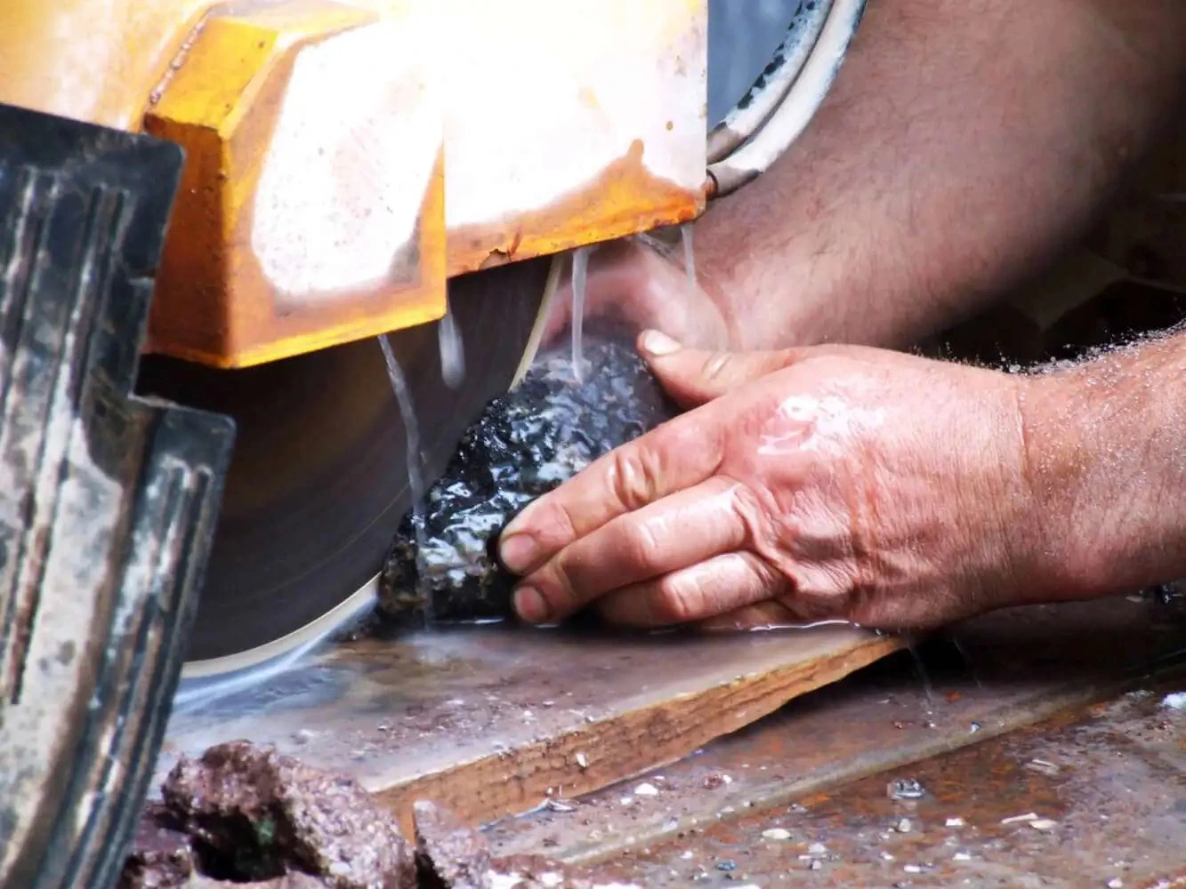
Dicing Blade Case Studies
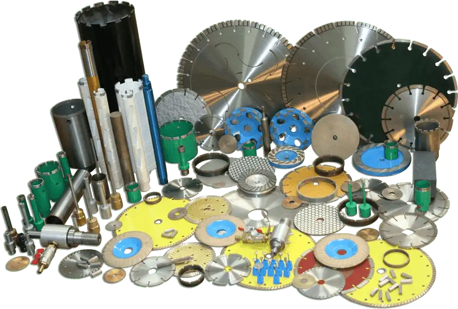
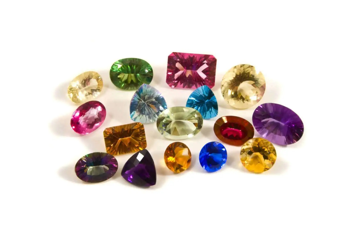
Selecting the right dicing blade is important to achieving high yields, superior edge quality, and consistent reliability in microelectronics and optics manufacturing. Across industries such as semiconductors, electronics packaging, photonics, and precision optics, even small...
27
Aug
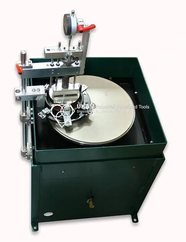
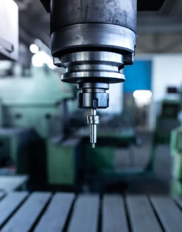
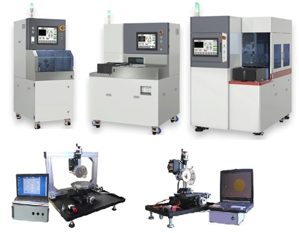
Selecting the Right Wafer Dicing Saw Practical Guide
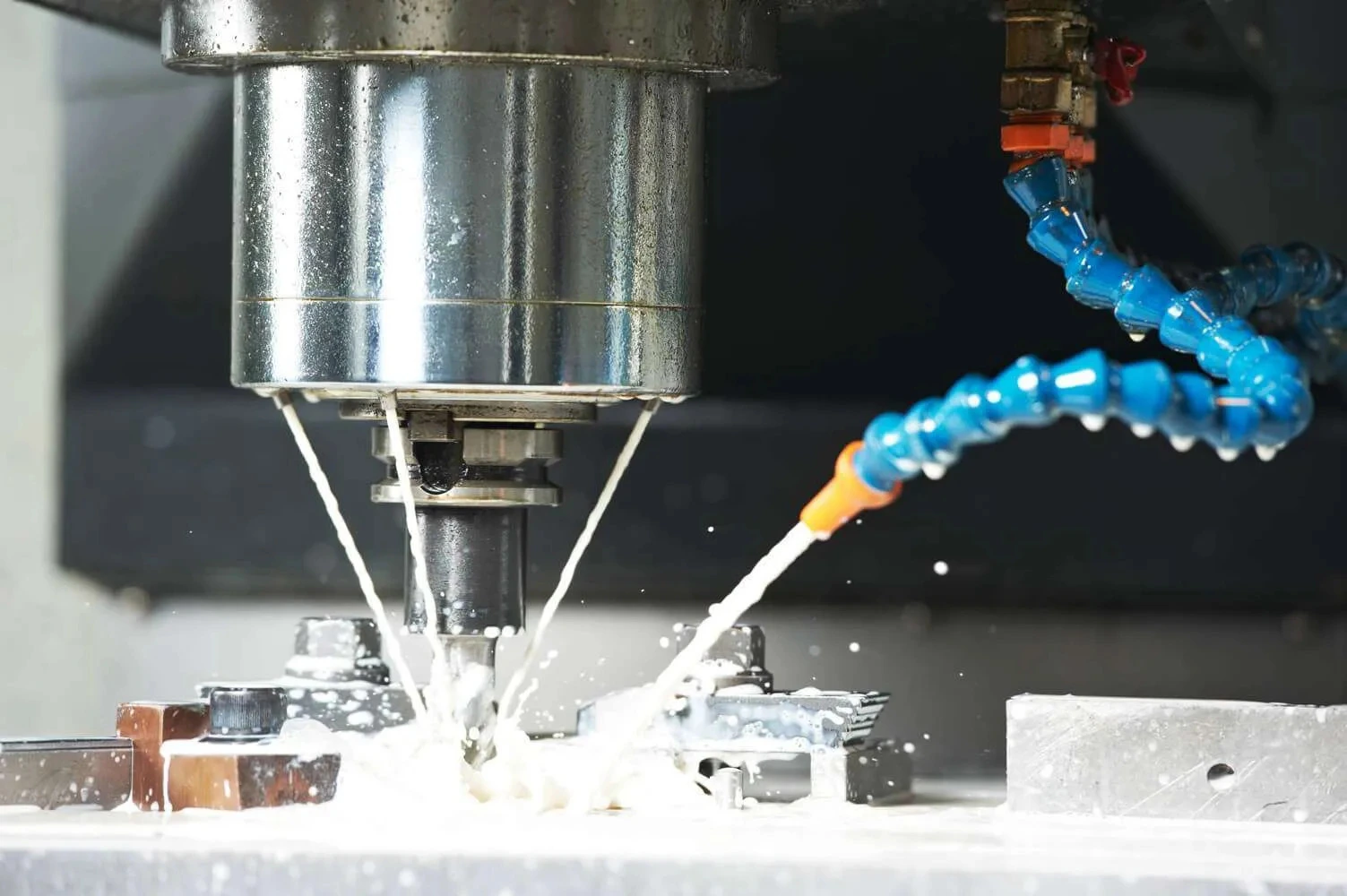
Selecting the proper wafer dicing saw is a important decision for manufacturers, researchers, and engineers working with large variety of materials. Whether processing silicon wafers in microelectronics, ceramics in materials science, or glass substrates in...
02
Sep
Practical Guide to Semiconductor Wafer Dicing: Materials, Blades, and Process Optimization
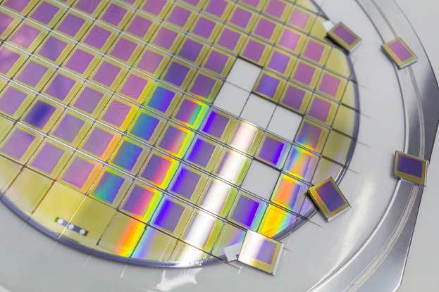
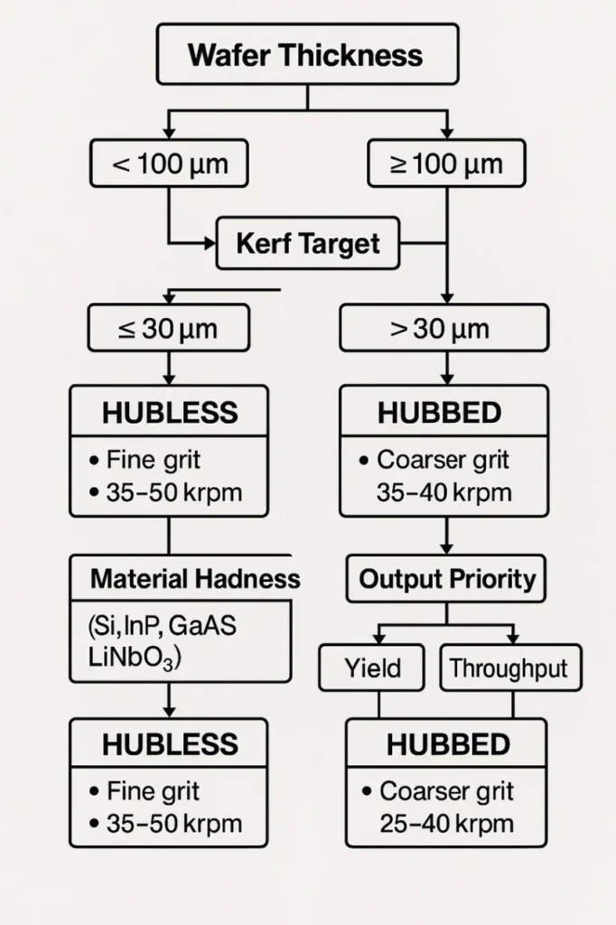
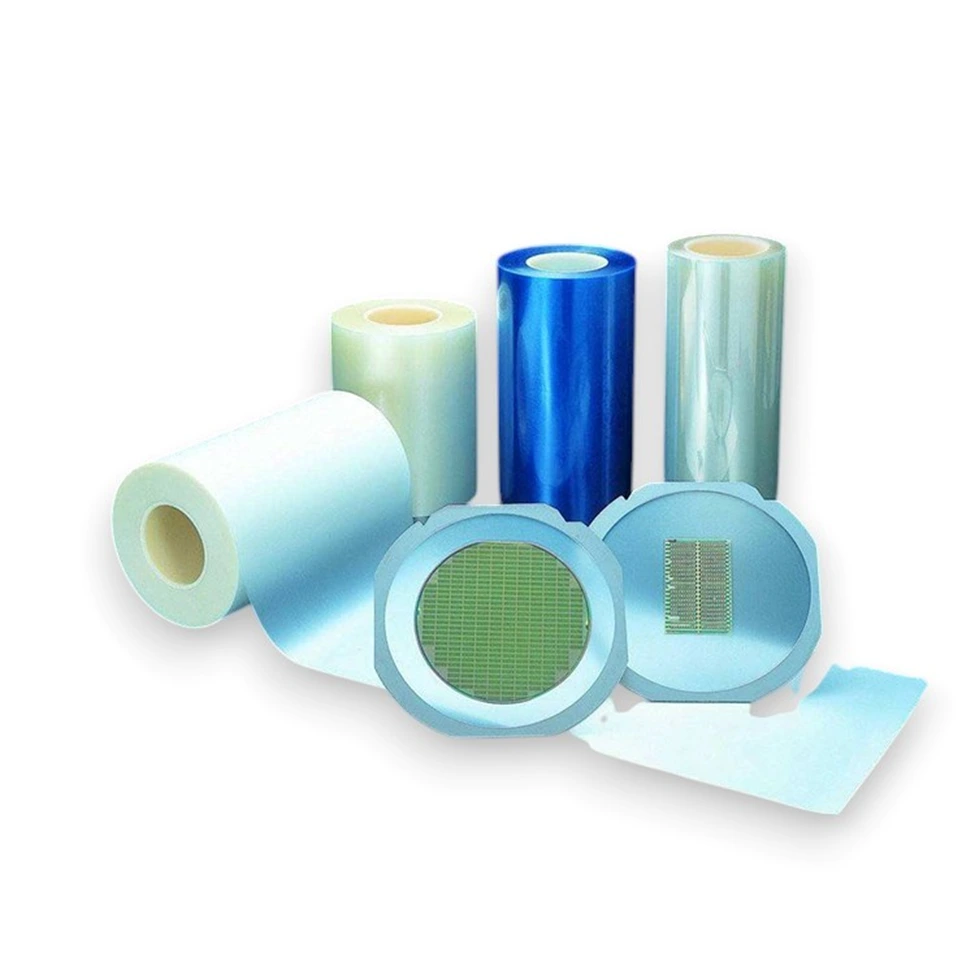
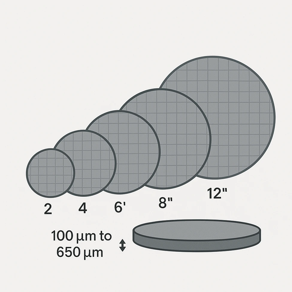
Semiconductor wafers are the foundation of nearly all modern electronics, from integrated circuits and photonic devices to advanced power components. As device geometries shrink and packaging density increases, the requirements placed on wafer dicing processes...