Silicon Fabrication Guide
-
Posted by
contactor6
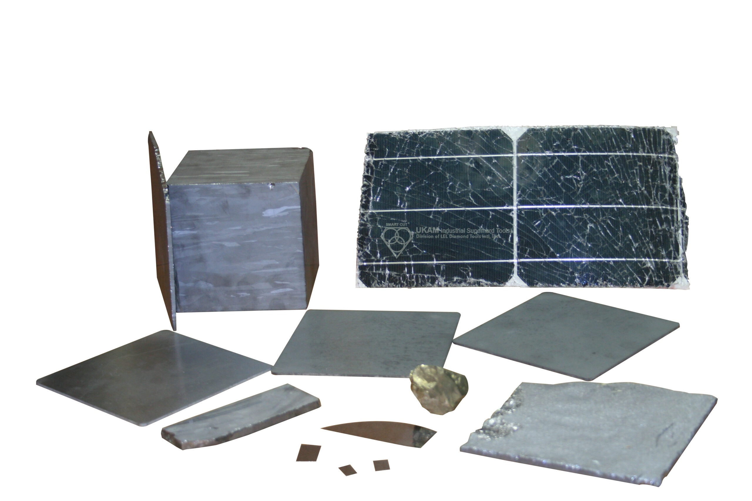
Cutting silicon wafers is a critical process in the manufacturing of semiconductor devices, where precision and control are paramount to the success of the final products. Silicon, a semi-metallic or metalloid, is the base material for most integrated circuits and solar cells, making its processing a cornerstone of the electronics and renewable energy industries. The cutting of silicon must be carefully managed to ensure that the integrity and purity of the wafers are maintained, as even minor imperfections can significantly impact the performance of the finished semiconductor devices.
This process involves several specialized techniques designed to slice, dice, and trim silicon into precise dimensions and shapes required for specific applications. Techniques such as ID sawing, wire sawing, and laser cutting are commonly employed, each offering unique benefits and suited for different requirements of thickness, surface finish, and production efficiency. These cutting methods must address challenges such as minimizing material loss, controlling heat generation, and preventing contamination.
As the demand for smaller, more powerful electronic devices continues to grow, the technology for cutting silicon has evolved to achieve greater levels of precision and efficiency. This introduction to silicon cutting explores the essential techniques and considerations involved in the process, providing a foundation for understanding the complexities and technicalities that ensure the high-quality production of silicon wafers essential for today's high-tech applications.
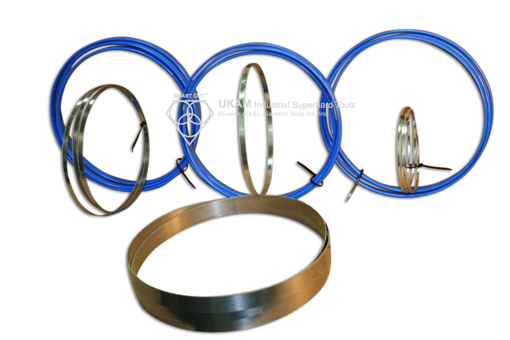
Cutting silicon wafers is a critical process in the manufacturing of semiconductor devices, where precision and control are paramount to the success of the final products. Silicon, a semi-metallic or metalloid, is the base material for most integrated circuits and solar cells, making its processing a cornerstone of the electronics and renewable energy industries. The cutting of silicon must be carefully managed to ensure that the integrity and purity of the wafers are maintained, as even minor imperfections can significantly impact the performance of the finished semiconductor devices.
This process involves several specialized techniques designed to slice, dice, and trim silicon into precise dimensions and shapes required for specific applications. Techniques such as ID sawing, wire sawing, and laser cutting are commonly employed, each offering unique benefits and suited for different requirements of thickness, surface finish, and production efficiency.
These cutting methods must address challenges such as minimizing material loss, controlling heat generation, and preventing contamination.
As the demand for smaller, more powerful electronic devices continues to grow, the technology for cutting silicon has evolved to achieve greater levels of precision and efficiency. This introduction to silicon cutting explores the essential techniques and considerations involved in the process, providing a foundation for understanding the complexities and technicalities that ensure the high-quality production of silicon wafers essential for today's high-tech applications.
Band Sawing
Diamond band sawing provides fast cutting rates and lower kerf loss on thicker material pieces. In band sawing the material is placed on the machine table which is movable and often powered by metered hydraulics, air over hydraulics, or stepper motors and ball screws.
The band is tensioned on a set of two or more running wheels, one of which is the driver. The work piece fixturing is similar to that required for table sawing. Find out more about diamond band saw blades >>>
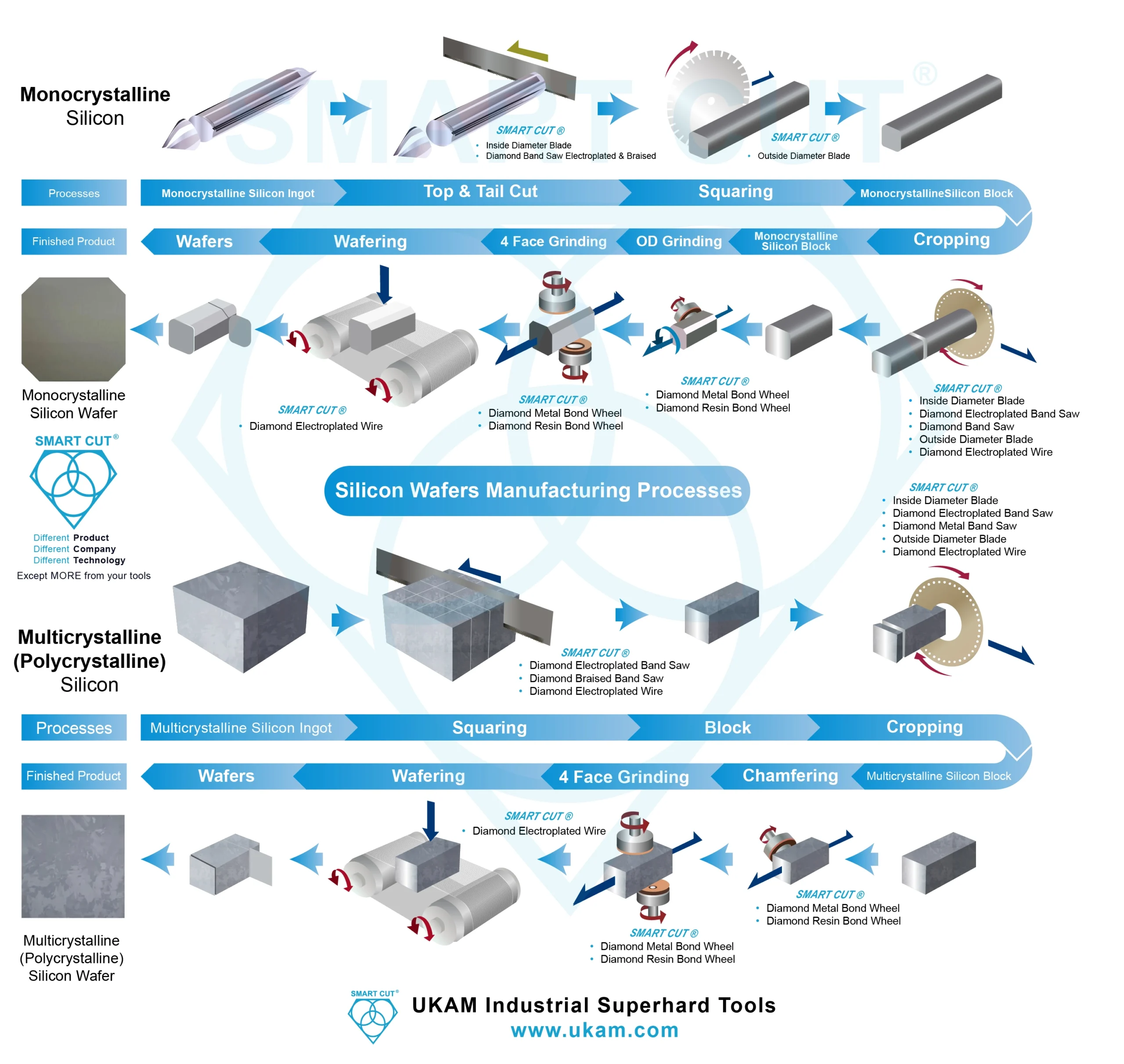
In solar wafer manufacturing the main purpose of band saws is to cut the incoming polycrataline or monocrytalline silicon ingots into bricks for desired wafer format.
There is a large variety of band saw machines available on the market. In the past while the solar silicon industry was still in its infancy, most manufacturers simply chose to convert band saw machines designed for metal working to be used with diamond band saw blades. Today, specialized band sawing equipment is available to meet the specific demands of solar silicon industry. Typically most diamond band saw blade thickness range from 0.5mm to 1.5mm. Kef loss varies from .040” to .080” depending on grit size of diamond particles and backing thickness. Specialized band saw machines for cutting solar silicon offer cutting band speeds up to 100 m/s and cutting accuracy for dimension variation perpendicularity and parallelism of + / - 0.2mm, less than 0.4mm and 0.3mm. Vertical travel on the band saw machine usually determines the height of the silicon ingot the can be processed. For example band saw machines with 20” wheels and larger allow sawing of silicon from ½” to 18” high and up to 24” long.
Typically the coarsest diamond grit size available for diamond band saw blades is 35/40 grit, and the finest is 180 grit. For rough cutting/squaring of silicon usually 60/80 grit is recommended. For final slicing/cropping finer grit size such as 100/120 mesh is recommended to produce finer cut and smoother surface finish quality.
High cutting rates can be produced with diamond band sawing in .1 to .2 cubic inches per minute when cutting silicon. The best surface finish that can be obtained with diamond band saw is about 32 RMS and usually requires secondary operations to obtain precise flatness and finish. The fast cutting rates combined with lower kerf loss on thicker material sections is one of the main advantages of diamond band saw process.
Some of the disadvantages include chip out at end of the cut, kerf (sludge) removal and machine war. Sludge of material debris develops after several hours of cutting. This requires use of filtering and settling techniques to remove this cutting waste. The chipping problem may be frequently resolved or minimized by use of waxed body at ed of the cut.
Band Slicing
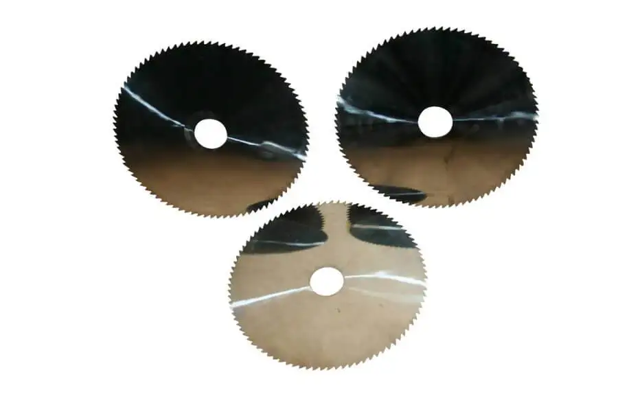
Kerf rates a s low as .012” can be obtained using diamond band saw slicing blades and techniques. Typically the diamond bands when mounted on sophisticated automatic indexing saws, can produce wafers comparable to ID annular sawing. Tolerances as close as .001” with no secondary finishing required.
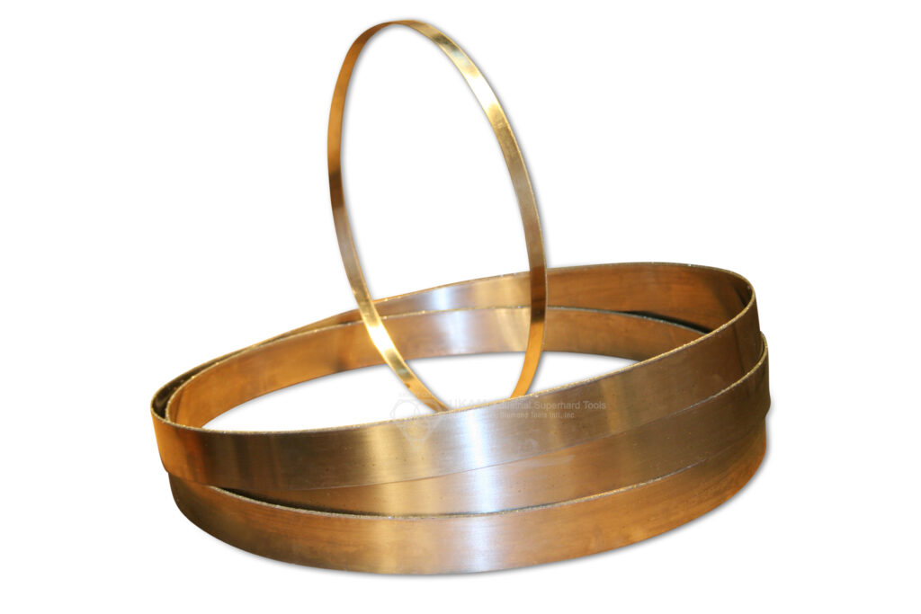
Top & Tail Cut" process for monocrystalline silicon (Cutting with Diamond Bands Saw Blade)
The band saw used in the "Top & Tail Cut" process for monocrystalline silicon is specifically designed to handle the hardness and brittleness of silicon ingots. The blade of the saw is crucial for achieving precise and clean cuts. It is typically made from a flexible steel band and meticulously coated with diamond particles either through electroplating or brazing. In electroplating, diamonds are bonded to the blade using a metal deposit, while brazing involves a higher-temperature process that creates a stronger bond between the diamonds and the blade, enhancing durability and cutting efficiency.
As the diamond band saw operates, it cuts through the silicon with a controlled motion that ensures minimal deviation and maximum precision.
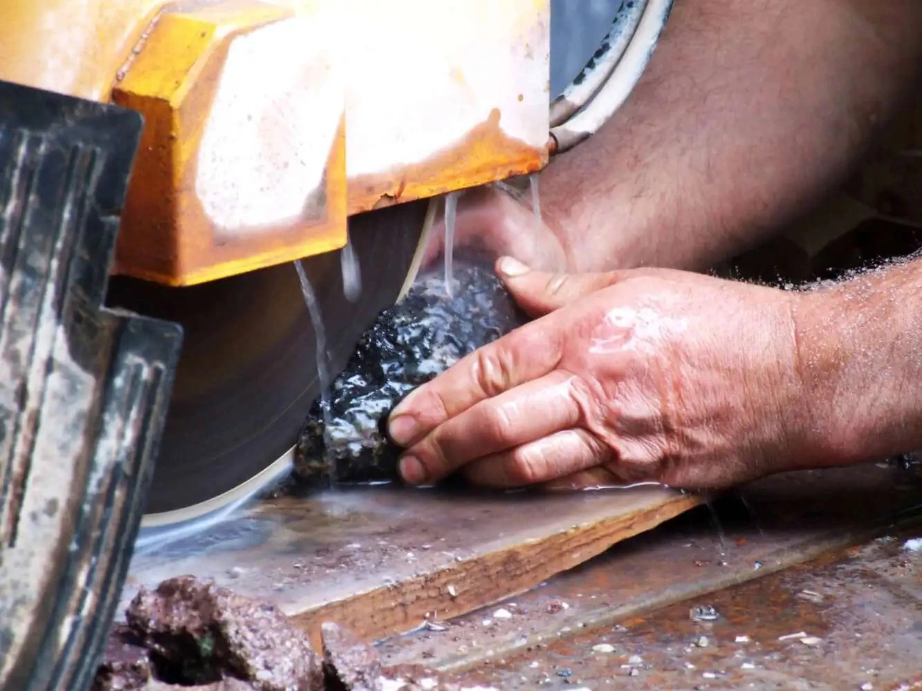
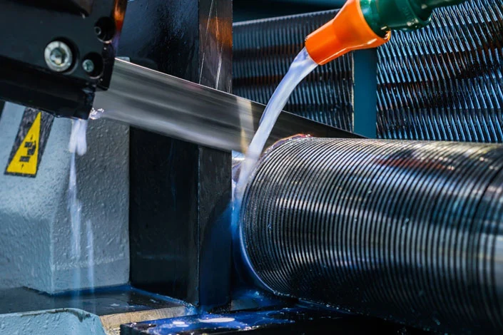
The speed and feed rate of the saw are optimized based on the properties of the silicon to prevent any damage to the crystal structure. Continuous cooling and lubrication are applied during the cutting process. This not only cools the blade and the ingot but also helps to wash away silicon particles and debris, preventing them from interfering with the cutting process and helping to extend the life of the blade.
Each cut is monitored to ensure it meets the stringent quality standards required for subsequent processing into silicon wafers. This careful monitoring and precise cutting capability make the diamond band saw an indispensable tool in the preparation of high-quality monocrystalline silicon for advanced applications in the semiconductor and solar industries.
The "Top & Tail Cut" process for monocrystalline silicon using a diamond band saw, while effective, presents several challenges that complicate its application in semiconductor and solar industries. The hardness of monocrystalline silicon exerts significant stress on the diamond-coated blades, leading to wear and tear. Despite the hardness of diamonds, the repetitive use and friction generated during cutting can degrade the blade's effectiveness, necessitating frequent replacements.
Maintaining the precision required for producing semiconductor-grade wafers is particularly challenging. Any deviation in the blade's path or inconsistency in speed can result in wafers that are not uniform in thickness or are damaged, impacting their utility in sensitive applications. Additionally, managing the heat generated during cutting is crucial; excessive heat can cause thermal damage to both the silicon ingot and the diamond blade, altering the properties of the silicon, inducing material stress, and reducing the overall quality of the wafers.
Material loss is also a significant concern. Some material is inevitably lost during the cutting process, which is a critical issue given the high value of purified monocrystalline silicon. Minimizing waste is essential for cost-efficiency but difficult to achieve. Ensuring that the cut surfaces are smooth and free from micro-cracks and other defects presents another major challenge. Such imperfections introduced during the cutting process can propagate during further processing, especially during high-temperature operations in wafer fabrication.
The process also generates silicon dust and debris that must be managed effectively. Accumulation of this debris can affect the cutting accuracy, damage the blade, and contaminate the silicon wafers, requiring sophisticated extraction and filtration systems. Furthermore, the operation involves high costs not only due to the use of diamond-coated blades but also because of the need for their regular replacement. The energy costs for running the cooling systems and the machinery itself add to the operational expenses.
Continuous quality control is required to ensure that each cut meets the stringent standards necessary for wafer production. This involves detailed inspections and can lead to high rates of product rejection if the wafers do not meet the required specifications. These challenges necessitate ongoing research and development to enhance blade technology, improve cutting techniques, and develop more effective cooling and debris management systems to meet the increasing demands for precision and efficiency.
Squaring Silicon using Diamond Band Saw Blades
Squaring is a critical operation in various industries requiring precision cutting. Diamond band saw blades are engineered to deliver precise, clean cuts in a variety of materials. These blades are coated with diamond particles, which are among the hardest known materials, making them ideal for cutting through hard substances such as ceramics, glass, stone, and various metals.
There are different types of diamond band saw blades, including diamond electroplated bands, diamond braised bands, and diamond electroplated wires. Diamond electroplated band saw blades have diamond particles electroplated onto the blade's surface, providing excellent cutting performance for a wide range of materials.
They are known for their sharpness and ability to maintain a high cutting speed. Diamond braised bands involve brazing diamond particles onto the blade, ensuring strong adhesion and long-lasting performance, particularly suited for more demanding cutting applications.
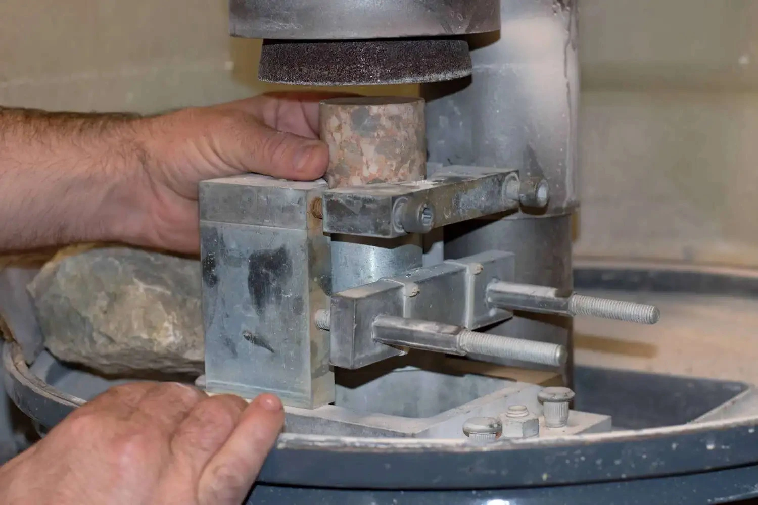
The squaring process involves cutting a material block into precise, square sections, which is crucial in applications requiring uniformity and exact dimensions, such as in the manufacturing of components for electronics, optics, and advanced ceramics. The material block to be squared is securely mounted on the cutting platform, ensuring that the block is properly secured to achieve accurate cuts and prevent movement during the cutting process. The appropriate type of diamond band saw blade is selected based on the material being cut. For example, harder materials may require a diamond braised band, while more delicate materials might be better suited to a diamond electroplated band. The band saw is set up with the selected blade, and the cutting parameters, such as speed, feed rate, and tension, are adjusted according to the material specifications and desired cut quality.
The saw is operated to make sequential cuts, ensuring that each cut is aligned to produce perfectly square sections. Precision and control are key factors during this step to achieve the desired dimensions and surface finish. After the cuts are made, the squared sections may undergo additional processes such as polishing, grinding, or inspection to meet specific quality standards.
Using diamond band saw blades for squaring offers several advantages. Diamond band saw blades provide extremely precise cuts with minimal chipping and deformation, essential for high-quality squaring operations. The cutting speed and efficiency of diamond blades reduce overall processing time, enhancing productivity. These blades can cut a wide range of hard and brittle materials, making them suitable for diverse industrial applications. The diamond coating ensures long-lasting blade life, reducing the frequency of blade changes and associated downtime.
The squaring process using diamond band saw blades is widely used in industries such as electronics, for cutting silicon wafers and other semiconductor materials; optics, for shaping optical components with precise dimensions; advanced ceramics, for producing high-precision ceramic parts used in various technical applications; and research and development, for material testing and sample preparation in laboratories. Using diamond band saw blades for the squaring process is a highly efficient and precise method for cutting hard materials into exact, square sections, essential in various high-tech industries where precision and quality are paramount.
The squaring process using diamond band saw blades faces several challenges that can impact its efficiency and precision. One significant challenge is ensuring the stability of the material block during cutting. Any movement or vibration can lead to inaccuracies, compromising the squareness and surface finish of the cut sections. Proper mounting and securing of the material are essential to address this issue, but it can be difficult, especially with irregularly shaped or fragile materials.
Selecting the appropriate diamond band saw blade for the specific material and cutting application is another challenge. Different materials require different types of blades, and using the wrong blade can result in poor cutting performance, increased wear, and potential damage to the material. Operators must have a thorough understanding of the material properties and blade characteristics to make the right choice.
Maintaining optimal cutting parameters, such as speed, feed rate, and tension, is critical for achieving precise cuts. However, these parameters can vary widely depending on the material and desired cut quality, making it challenging to set and adjust them correctly. Inadequate control over these parameters can lead to excessive wear on the blade, increased chipping, and uneven cuts.
Blade wear and maintenance present ongoing challenges. Diamond band saw blades, although durable, eventually wear out and require replacement. Monitoring blade condition and performing timely maintenance is crucial to ensure consistent cutting quality. Failure to do so can result in subpar performance and increased production downtime.
Another challenge is managing the cooling and lubrication during the cutting process. Proper cooling helps to dissipate heat generated by the cutting action, preventing damage to both the blade and the material. Insufficient cooling can lead to overheating, causing thermal damage and reducing blade life. Maintaining an adequate and consistent supply of coolant or lubricant is essential but can be logistically complex.
Handling the cutting debris and ensuring a clean cutting environment is also important. Debris accumulation can interfere with the cutting process, leading to poor cut quality and increased wear on the blade. Effective debris management, including using appropriate extraction systems and cleaning protocols, is necessary to maintain a smooth operation.
Lastly, achieving consistent cut quality across multiple sections is a challenge. Variations in material properties, blade condition, and cutting parameters can lead to inconsistencies in the final product. Continuous monitoring and adjustments are required to ensure that each cut meets the desired specifications, which can be time-consuming and require skilled operators.
Cropping Silicon Using Diamond Band Saw Blades
Using diamond band saw blades for cropping involves several key steps. First, the workpiece is securely mounted on the cutting platform to prevent any movement during the cutting process. Proper mounting is critical to ensure accuracy and consistency in the cuts. The appropriate type of diamond band saw blade is then selected based on the material being processed. For instance, electroplated diamond blades are known for their sharpness and speed, making them suitable for softer or more delicate materials, while braised diamond blades offer stronger adhesion and durability for harder materials.
Once the blade is selected and installed, the cutting parameters such as speed, feed rate, and tension are set according to the material's characteristics and the desired outcome.
These parameters are crucial for achieving clean and precise cuts. During the cutting operation, the saw is carefully guided to remove the excess material, following the predetermined cutting path. Precision and control are paramount to avoid any deviation from the desired dimensions.
Throughout the cropping process, proper cooling and lubrication are maintained to dissipate the heat generated by the cutting action. This prevents overheating, which can damage both the blade and the material. Adequate cooling also extends the blade's life and ensures a smooth cutting process.
Debris management is another important aspect of the cropping process. As the blade cuts through the material, debris is generated, which can interfere with the cutting operation if not properly managed. Effective debris extraction systems and regular cleaning help maintain a clear cutting path and consistent cut quality.
Blade wear and maintenance are ongoing concerns in the cropping process. Regular monitoring of the blade condition and timely maintenance are essential to sustain cutting performance. Worn blades need to be replaced to avoid compromising the quality of the cuts.
The cropping process using diamond band saw blades offers several advantages, including high precision, efficiency, and the ability to handle a wide range of materials. However, it also presents challenges such as ensuring material stability, selecting the appropriate blade, optimizing cutting parameters, maintaining cooling and lubrication, managing debris, and monitoring blade wear. Addressing these challenges effectively is crucial for achieving optimal results in industrial applications.
The cropping process using diamond band saw blades faces several challenges that can impact its efficiency and precision. One significant challenge is ensuring the stability of the workpiece during cutting. Any movement or vibration can lead to inaccuracies, compromising the dimensional precision and surface finish of the cropped sections. Proper mounting and securing of the workpiece are vital to address this issue, but it can be difficult, especially with irregularly shaped or fragile materials.
Selecting the appropriate diamond band saw blade for the specific material and cropping application is another challenge. Different materials require different types of blades, and using the wrong blade can result in poor cutting performance, increased wear, and potential damage to the material. Operators must have a thorough understanding of the material properties and blade characteristics to make the right choice.
Maintaining optimal cutting parameters, such as speed, feed rate, and tension, is critical for achieving precise cuts. However, these parameters can vary widely depending on the material and desired cut quality, making it challenging to set and adjust them correctly. Inadequate control over these parameters can lead to excessive wear on the blade, increased chipping, and uneven cuts.
Blade wear and maintenance present ongoing challenges. Diamond band saw blades, although durable, eventually wear out and require replacement. Monitoring blade condition and performing timely maintenance is crucial to ensure consistent cutting quality. Failure to do so can result in subpar performance and increased production downtime.
Another challenge is managing the cooling and lubrication during the cutting process. Proper cooling helps to dissipate heat generated by the cutting action, preventing damage to both the blade and the material. Insufficient cooling can lead to overheating, causing thermal damage and reducing blade life. Maintaining an adequate and consistent supply of coolant or lubricant is essential but can be logistically complex.
Handling the cutting debris and ensuring a clean cutting environment is also important. Debris accumulation can interfere with the cutting process, leading to poor cut quality and increased wear on the blade. Effective debris management, including using appropriate extraction systems and cleaning protocols, is necessary to maintain a smooth operation.
Achieving consistent cut quality across multiple sections is a challenge. Variations in material properties, blade condition, and cutting parameters can lead to inconsistencies in the final product. Continuous monitoring and adjustments are required to ensure that each cut meets the desired specifications, which can be time-consuming and require skilled operators.
Oscillating Wire Slurry & Diamond Wire Saws
Wire saws provide the most accurate cutting with the least amount of surface damage and chipping of material. Find out more about diamond wire >>>
Today wire sawing is preferred by majority of solar silicon manufacturers over other technologies/cutting methods. Wire saw operates similarly to horizontal hack saw, where head containing a pack of blades lengths of plain edge stainless or spring steel mounted parallel to head travel oscillates back and forth over the work piece or pieces which are mounted on a bed. The bed can be fed up into the blades at selected pressures. A series of nozzles apply a flow of abrasive slurry (grains of silicon carbide or other abrasive in a liquid vehicle.
That provide a cutting or lapping action between the blades and material. The wire saw allows slicing of hundreds of wafers simultaneously with the same continuous wire. For the most part today abrasives are used and preferred over diamond for cutting silicon.
Although use of wire bonded with diamond offers many advantages in terms of faster cutting speed (frequently triple the speed) and improved surface finish quality (less secondary operations such as polishing). Due to the pullouts of diamond crystals/particles, the cutting life is short and costly for high production scenario.
For this reason, most silicon manufacturers utilize copper plated piano wires designed to trap abrasive particles (such as alumina or SiC) suspended in mechanical oil or water based coolant. To provide the cutting action and lubrication of the moving wire. The wire diameter frequently used is smaller than 0.15mm and cutting kerf is about 0.19mm and 0.15mm and smaller. Abrasive slurry grit size varies from 1000 to 250 grit. Viscosity and continuous mixing of the slurry must be maintained in order to produces consistent results.
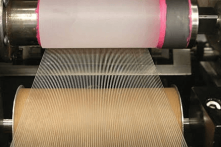
Wire is would around 2, 3,or 4 grooved mandrels in order to allow multiple loops for simultaneous slicing of the same ingot. When the looped wire is running across the ingot, the abrasive particles impeded the soft surface of the piano wire will slowly lap/grind off silicon on micro level (bit by bit). The cutting action is done by reciprocating motion. The wire is used once, and replaced with a new roll.
Typically this type of wire saw can travel at surface speed of 6 mm/sec. The wire moves forward for abut 300mm and this is retraced for abut 200mm. Net advance of the new wire is at an average speed of 2 m/sec with about 100 m new wire passed through each cycle. The wire can run continuously for more than 300 km long. More than 500 slices can be sawn simultaneously. In a production environment 8” (200mm) silicon boul in leas than 8 hours and 12” (300mm) boul in less than 12 hours.
wafering of monocrystalline and polycrystalline silicon
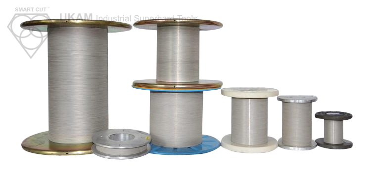
The wafering of monocrystalline and polycrystalline silicon is a critical step in the production of silicon wafers. This process involves slicing large blocks of silicon into thin wafers, which are subsequently processed to fabricate semiconductor devices or solar cells. The image likely depicts the use of a diamond electroplated wire saw, a popular choice for this application due to its precision and efficiency.
Diamond wire sawing is a critical technique in the wafering of both monocrystalline and polycrystalline silicon, extensively utilized in the semiconductor and solar industries to produce high-quality wafers. This method uses a wire embedded with diamond particles, typically bonded through an electroplating process, to perform precise cuts while minimizing material loss and enhancing production efficiency.
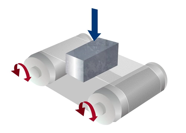
In the setup phase, the silicon ingot is mounted securely on the slicing equipment, and the diamond wire is threaded through a series of precisely aligned guides. It is then tensioned to maintain its stability and ensure it remains straight and accurate during the cutting process. The wire saw operates by propelling the wire across the ingot in a continuous, fast-moving loop driven by pulleys or wheels. This enables the wire to slice through the silicon block efficiently.
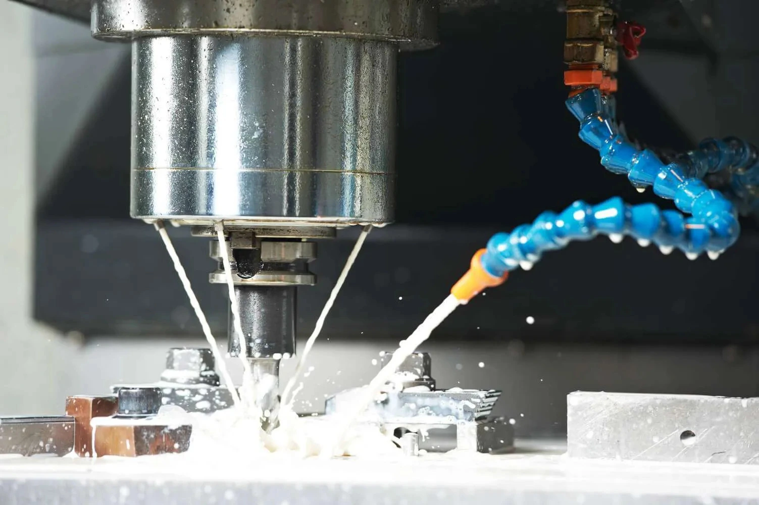
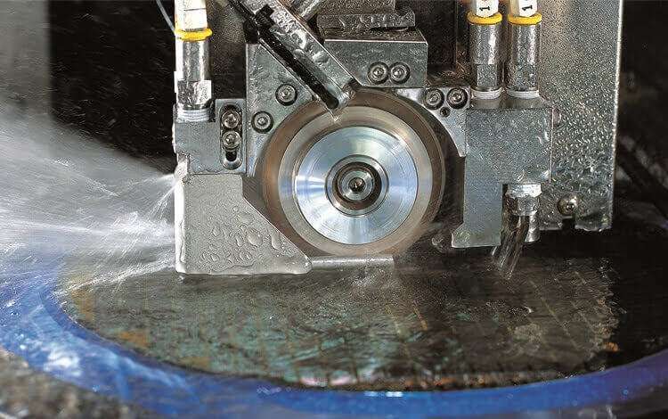
During the cutting process, a constant stream of coolant is applied to prevent overheating of both the wire and the material. This cooling is crucial as it also helps flush away silicon dust and debris, which could otherwise impair the cutting efficiency or damage the wire.
The advantages of using diamond wire for slicing silicon include precision and control, which allow for the production of wafers at very controlled thicknesses, essential for the functional consistency of semiconductor devices and solar cells.
The technique produces a thin kerf, significantly reducing material wastage—a vital benefit given the high cost of silicon. Diamond wire sawing is also faster than traditional methods like slurry saws, enabling higher production volumes in shorter times.
The surface finish of wafers sawn with diamond wire is generally superior, reducing the need for extensive post-processing. This efficiency reduces overall manufacturing time and costs. Moreover, the adaptability of the diamond wire sawing process makes it suitable for both monocrystalline and polycrystalline silicon. Monocrystalline silicon, used in high-efficiency applications, benefits particularly from the minimal kerf loss and high surface quality, while the slightly lower quality requirements of polycrystalline silicon are easily met with the same equipment.
Wafering monocrystalline and polycrystalline silicon using diamond wire, despite its efficiency and precision, involves several challenges that can complicate the manufacturing process and affect output quality.
Firstly, achieving consistent quality in diamond wire itself is a significant challenge. Variations in the diamond coating, such as inconsistency in grain size or density, can lead to uneven wear and tear during cutting, affecting the quality of the wafers. Manufacturers must ensure that the diamond wire used is of high quality and consistently manufactured to avoid these issues.
Another major challenge is optimizing the cutting parameters, including wire speed, tension, and the volume and type of coolant used. These parameters must be precisely controlled to maximize cutting efficiency and minimize damage to the wafers. Incorrect settings can lead to wire breakage, excessive material loss, or suboptimal wafer surface quality, necessitating costly post-processing.
Wire breakage is a frequent issue and can cause significant disruptions in production. It often results from mechanical stress or from the wire becoming worn out. Regular monitoring and replacing of the wire is required to prevent unexpected downtime, which can be costly both in terms of production delays and material wastage.
Cooling and debris removal also pose challenges. The cutting process generates heat and silicon debris, which must be effectively managed with appropriate coolant systems. If cooling is insufficient, it can lead to overheating, which affects the structural integrity of the silicon wafers. Moreover, the spent coolant and debris need to be handled and disposed of in compliance with environmental standards, adding to the operational complexities.
Integrating diamond wire technology into existing systems involves substantial setup costs and technical adjustments. This technology typically requires significant upfront investment in specialized equipment and training for personnel, which can be a barrier for smaller operations or those with limited capital.
Lastly, maintaining production efficiency while managing these challenges is crucial for the economic viability of using diamond wire in wafering processes. Manufacturers need to balance the high initial and ongoing costs with the benefits of increased yield and reduced kerf loss to determine the practicality of adopting this technology in their operations.
Implementation of Diamond Wire Sawing in Solar Panel Manufacturing
Background: A leading solar panel manufacturer transitioned from traditional slurry-based saws to diamond wire sawing to slice polycrystalline silicon ingots into wafers.
Implementation: The manufacturer upgraded their production line to incorporate advanced diamond wire sawing machines capable of handling multiple ingots simultaneously. The wire used was a 140-micron thick diamond electroplated wire, optimized for high-speed cutting and minimal kerf loss.
Results
-
 Yield Improvement: The thinner kerf of the diamond wire reduced silicon waste by approximately 30%, significantly increasing the number of wafers obtained per ingot.
-
 Cost Reduction: Operational costs were reduced by 20% due to lower material waste and decreased need for blade replacements, as diamond wires have a longer lifespan compared to traditional blades.
-
 Production Speed: Sawing time was reduced by 40%, enabling faster production cycles and increased throughput.
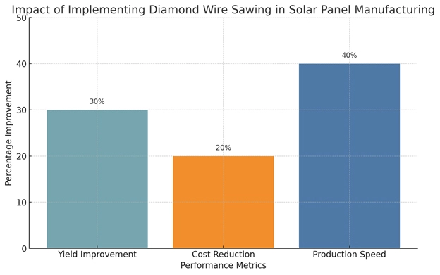
Conclusion: The switch to diamond wire sawing provided substantial cost savings, improved material utilization, and enhanced production efficiency, making it a crucial step in maintaining competitiveness in the solar industry.
Case Study 2: Upgrading to Diamond Wire Technology in Semiconductor Wafer Fabrication
Background: A semiconductor company specializing in the production of monocrystalline silicon wafers implemented diamond wire sawing to enhance their wafer production line.
Implementation: The company introduced a precision-controlled diamond wire sawing system designed for the delicate slicing of monocrystalline silicon, focusing on maintaining the integrity of the crystal structure.
Results
-
 Increased Precision: The use of diamond wire sawing allowed for more precise cuts, which is critical in semiconductor manufacturing, resulting in higher quality wafers with uniform thickness.
-
 Reduction in Material Loss: The thin diamond wire reduced kerf loss by 25%, increasing the total output of usable wafers and reducing raw material costs.
-
 Enhanced Surface Quality: Wafers required less post-cut polishing, reducing processing time and labor costs associated with the wafer finishing phase.
Conclusion: Diamond wire sawing not only streamlined the production process but also enhanced the quality of the wafers produced, leading to higher yields and lower production costs, crucial for maintaining an edge in the highly competitive semiconductor market.
Ingot Slicing
The use of diamond wire in ingot slicing is a highly specialized method for producing wafers, especially effective for materials such as silicon or sapphire. Diamond wire saws have significantly enhanced the efficiency and quality of the slicing process compared to traditional methods.
Diamond wire is composed of a thin, flexible wire base, usually made of steel, coated with a layer of diamond grains. These diamonds are typically bonded to the wire via electroplating, and they serve as the cutting abrasives that slice through the ingot material as the wire is drawn across it.
In the cutting process, the ingot to be sliced is securely mounted on the cutting apparatus, and the diamond wire is threaded through a series of guides and tensioned to ensure stability during cutting. The wire saw operates by moving the diamond-coated wire across the ingot at a controlled speed, in a continuous loop around drive wheels, similar to a band saw. This setup maximizes cutting speed and efficiency.
Throughout the slicing process, a coolant or lubricant is applied to prevent overheating and to remove material debris. This cooling process is crucial as it also preserves the life of the diamond wire by minimizing wear and tear.
The advantages of using diamond wire for ingot slicing include achieving very precise and thin cuts, which significantly reduces material wastage. This method produces cleaner cuts with fewer surface defects, reducing the need for extensive post-cutting surface treatment. It also allows for faster processing speeds, increasing throughput while maintaining the quality of the wafers.
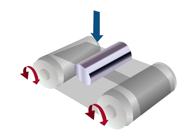
Diamond wire is versatile enough to slice various materials, including hard or brittle substances like sapphire, as well as delicate materials without causing significant damage. Although the initial setup costs can be high, the increased productivity and decreased material loss result in a lower cost per wafer over time.
Diamond wire sawing, while offering numerous advantages in the wafering of silicon and other hard materials, also presents several challenges that can impact operational efficiency, product quality, and economic viability.
One of the primary concerns is wire breakage and the need for frequent maintenance. Diamond wire saws are susceptible to wire breakage due to excessive tension, rapid wear, or mechanical failures in the wire driving system. Regular maintenance and monitoring are required to ensure the integrity of the wire and the machinery, which can increase operational costs and necessitate skilled technicians.
The quality of the diamond wire itself can also vary, affecting the consistency of cuts and the overall quality of the wafers. Variations in diamond size, distribution, and bonding strength can lead to inconsistent performance. Ensuring a consistent supply of high-quality diamond wire involves finding reliable suppliers and can be costlier, impacting the overall production budget.
Optimizing cutting parameters such as wire speed, tension, and cooling rates for different materials and ingot sizes presents another layer of complexity. Incorrect parameters can lead to inefficient cutting, increased material waste, or damage to the wafers. Continuous investment in research and development is required to refine these parameters, which demands significant resources.
Effective cooling is crucial to prevent overheating of the wire and the material, which can affect cut quality and lead to potential mechanical failures. Managing the coolant flow and composition to ensure it effectively removes heat and debris without causing contamination is challenging. Additionally, the process generates significant waste, including spent coolant and silicon dust, which must be disposed of in accordance with environmental regulations, adding to operational costs.
Integrating diamond wire sawing technology into existing production lines can require substantial modifications in machinery and processes. This adaptation can be costly and time-consuming. Training staff to operate and maintain new sawing equipment is crucial for efficient operation. Skilled operators are essential to manage the sophisticated equipment and optimize production efficiency.
Lastly, the initial investment for setting up diamond wire sawing equipment can be significant, posing a substantial financial decision, particularly for smaller manufacturers. While the long-term benefits of reduced material wastage and increased production efficiency can justify this investment, the upfront costs and ongoing maintenance expenses can be a barrier to entry for some companies.
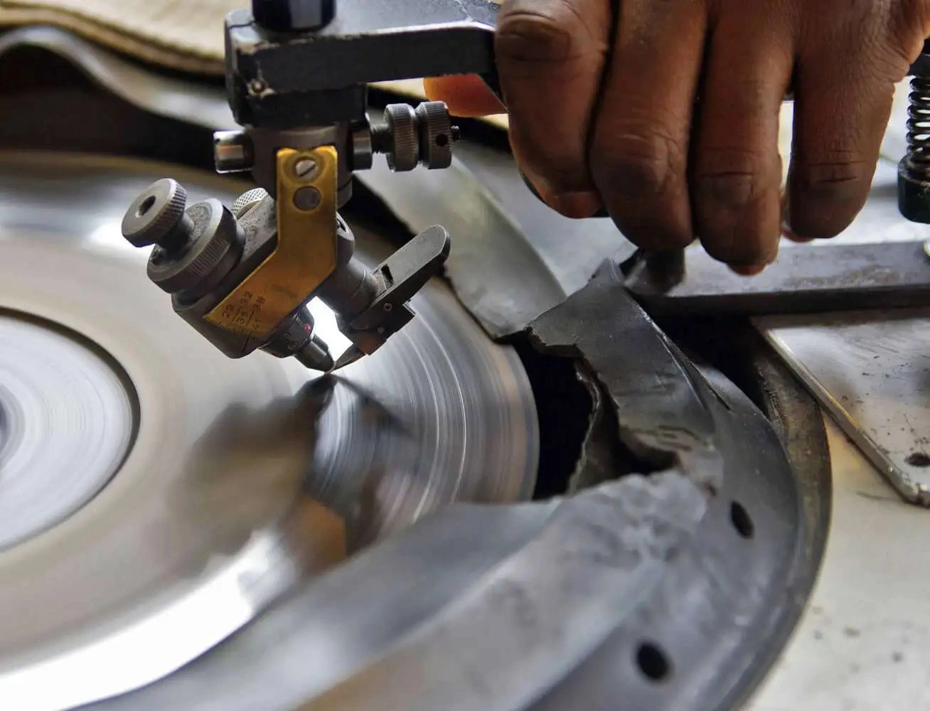
ID sawing
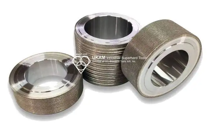
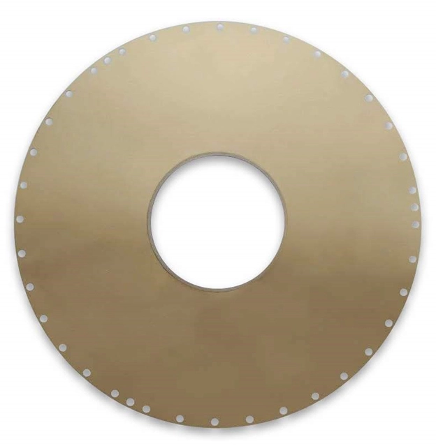
The tension of the blade is provided by the strength to resist deflection during sawing with only a fraction of the cross section of peripheral wheels. A single layer of very fine diamond powder in range of 150 to 600 mesh is bonded to the leading edge of the pening and roughly 1/8” down each side by diamond deposition method. Find out more about Inside Diameter Diamond Blades >>>
The silicon material workpeice is suspended inside the opening and then accurately fend into the cutting edge. The fixture remains rigid yet gives up wafers freely after they have been sliced. Typically for this application the silicon ingots are mounted on inexpensive disposable carbon bars with a low temperature non loading wax or epoxy.
ID blades limit the size of the silicon work piece by design. The material must be small enough to fit into the opening. , while the distance from the cutting edge to the mounting ring determines the depth of cut. When the diameters of silicon ingots used to be smaller than 8 inches, this cutting method was the industry standard for many years. Allowing high cutting efficiency. The 8” silicon ingot could be typically cut within ten minutes. However, with increased diameter of silicon ingots used today such as 8” to 12”. The industry has for the most part moved away from ID sawing because the thin blade cannot support the distance of cutting. At the same time inside diameter diamond blades can cut only one slice at time, and do not have the cutting efficiency and sped as wire saws.
Cropping Silicon Using Inside Diameter Blades
The cropping process in industrial settings often involves resizing or sectionalizing materials into more manageable or specifically sized pieces using industrial diamond blades. These blades are favored for their precision and ability to handle a variety of materials, including ceramics, metals, composites, and advanced materials.
Industrial diamond (ID) blades are chosen for their exceptional hardness, which allows them to cut through tough materials with minimal wear. Their cutting edges are embedded with synthetic diamond grit, which provides a combination of sharpness and durability essential for efficient cropping. The advantages of using ID blades include precision cutting, which produces cleaner cuts with tighter tolerances than conventional blades; reduced material waste, which is crucial when working with expensive materials; enhanced cutting speed, as diamond blades can operate at higher speeds without sacrificing cut quality; and versatility, as they can handle a variety of materials from soft aluminum to hard quartz or ceramics.
When using ID diamond blades for cropping, it's important to consider several factors to optimize the process. The choice of blade should be suited to the material type and desired cut quality, with considerations for diamond grit size, concentration, and the matrix material. The cutting machine should be capable of handling the size and type of blade and provide the necessary power and stability. Adjusting the feed rate to match the material’s hardness and thickness is crucial; too fast a feed rate can cause blade overheating and wear, while too slow can reduce efficiency. Using appropriate coolants can prevent overheating and remove debris from the cutting area, affecting both cut quality and blade life. Regular checks for blade wear and tear are necessary, as even high-quality diamond blades deteriorate and require dressing to restore their cutting performance.
To achieve optimal results during the cropping process with ID diamond blades, technical specifications such as RPM (rotations per minute), blade diameter, and cutting depth must be precisely aligned with the material properties and the desired outcomes. For instance, cropping a piece of sintered carbide, a very hard material, would ideally be done using a thin kerf diamond blade with a fine grit size for a smooth surface finish. The machine's RPM should be adjusted to the lower end of the blade's capability to minimize the risk of chipping the carbide, and coolants should be used to keep the cutting zone clean and cool, enhancing the blade's lifespan and the quality of the cut.
Dicing Silicon for semiconductor devices
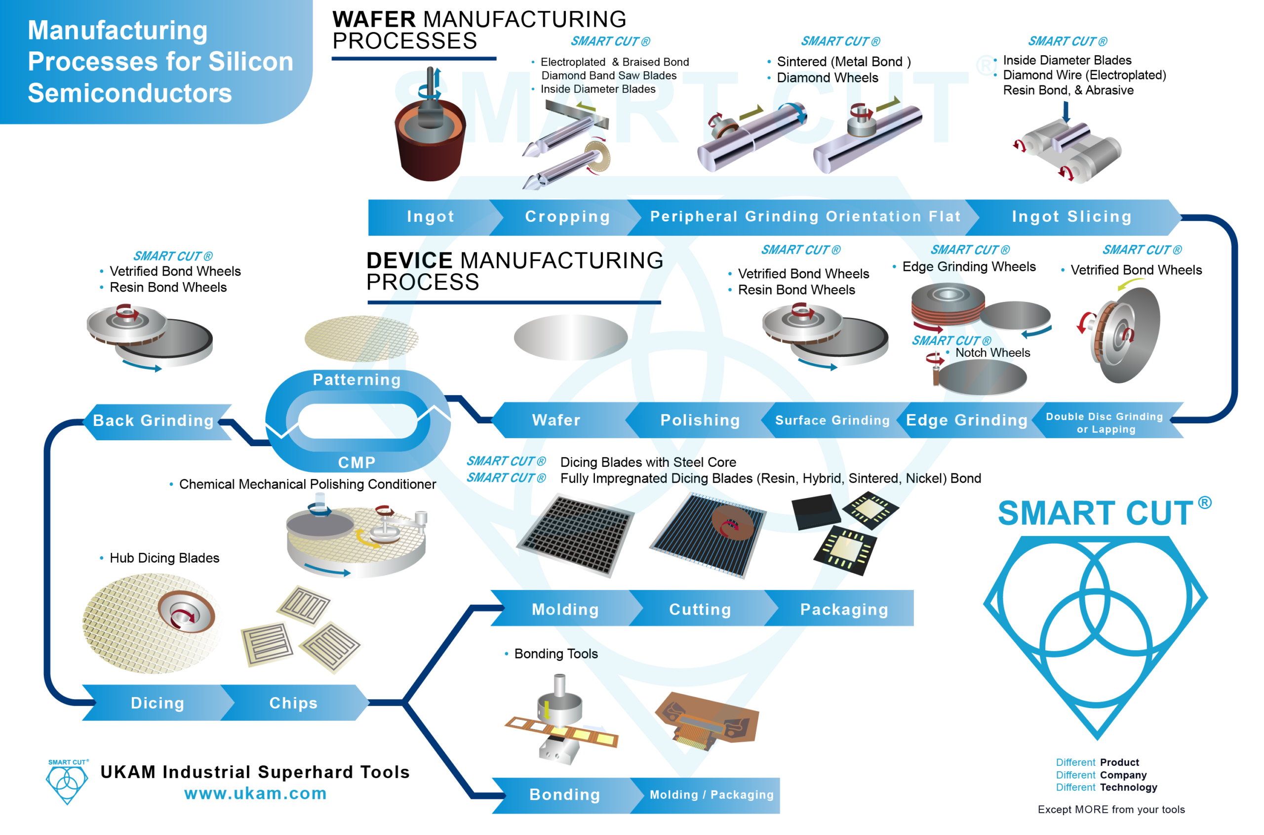
Dicing is a crucial step in the fabrication of semiconductor devices, where a full silicon wafer is segmented into individual chips, also known as die. This process must be precisely controlled to ensure that the integrity and functionality of each die are maintained. The choice of dicing blades and techniques significantly impacts the quality, efficiency, and cost of semiconductor production. Find out more about dicing blades >>>
Resin bond blades are commonly used because they provide smooth cuts with minimal chipping, thanks to their diamond abrasives held together by a resin binder. The flexibility of the resin bond allows for high-speed cutting with reduced mechanical stress on the wafer, ideal for materials sensitive to cracking and chipping. Hybrid bond blades combine resin and metal bonds to offer the benefits of both materials, providing a balance between cut quality and blade life. These blades are effective for hard and brittle materials, enhancing cutting ability with less wear. Sintered nickel bond blades, made by sintering diamond particles in a metal matrix, typically nickel, are extremely durable and maintain a sharp cutting edge over extended periods. These blades are useful for high-volume production where longevity and consistent cutting depths are critical.
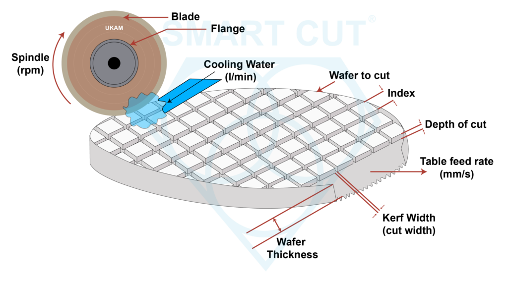
Various dicing techniques are employed depending on the material of the wafer and the desired outcomes. Blade dicing, the most common method, involves a rotating diamond-coated blade cutting through the wafer and is preferred for its speed and efficiency in high-volume settings. Stealth dicing, a newer technique, uses a laser to create a modified layer within the wafer, allowing it to be broken apart with minimal physical stress and is advantageous for very thin or brittle materials. Laser dicing, which uses lasers to cut the wafer, offers high precision and flexibility in cutting paths and is useful for complex shapes or when minimal damage to the surrounding material is critical.
Dicing silicon wafers presents several challenges, including kerf loss—the width of the cut made by the blade—which results in material loss. Minimizing kerf width is crucial to maximizing the number of dies per wafer. Both blade and laser dicing can generate significant heat, which may cause damage to the die or affect its properties. Managing heat through optimal blade speed and coolant use, or by adjusting laser parameters, is essential. Mechanical stresses during dicing can lead to chip edges chipping off or entire dies cracking. Using appropriate blade types and cutting parameters is key to minimizing these defects.


