Manufacturing Processes for Silicon Semiconductors From Ingot to Integrated Circuit
-
Posted by
contactor6
1. Ingot Production
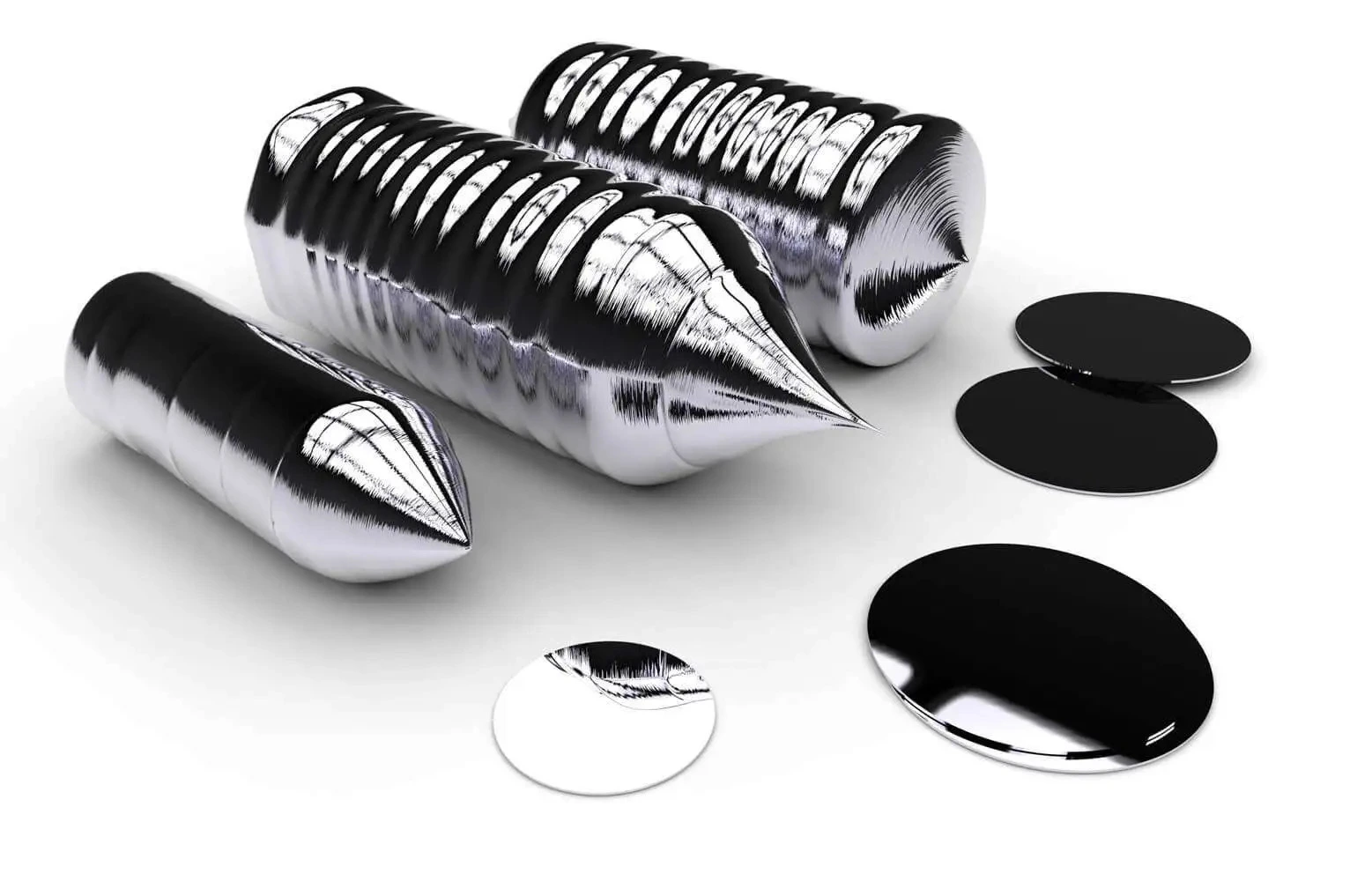
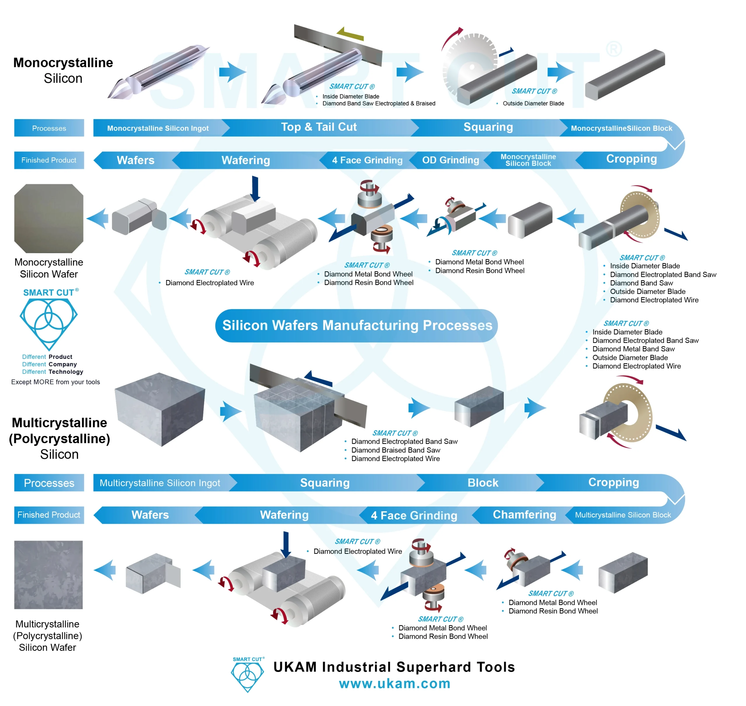
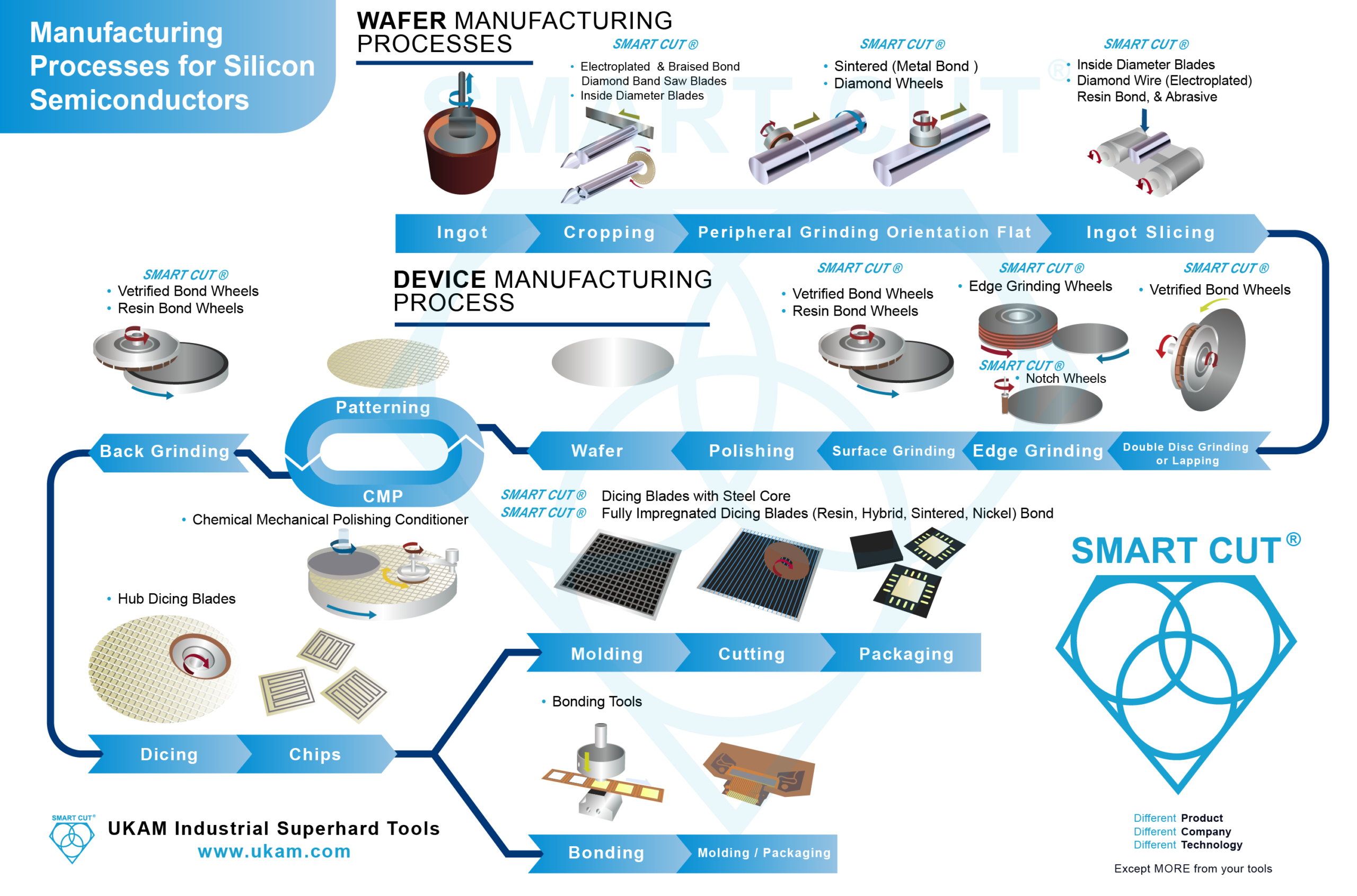
The journey begins with the creation of silicon ingots, which are pure silicon cylinders produced through methods like the Czochralski process. Once formed, these ingots undergo a cropping procedure to remove any excess and to prepare them for slicing. This step ensures that only the highest quality silicon is used, which is crucial for the performance of the final semiconductor devices.
2. Ingot Cropping
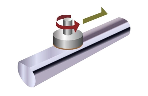
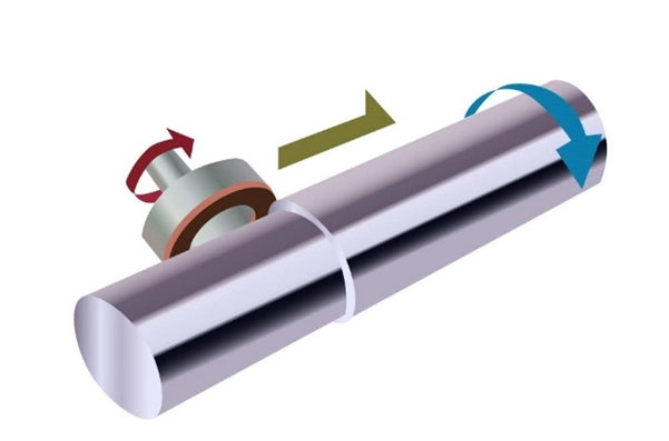
3. Peripheral Grinding and Orientation Flat
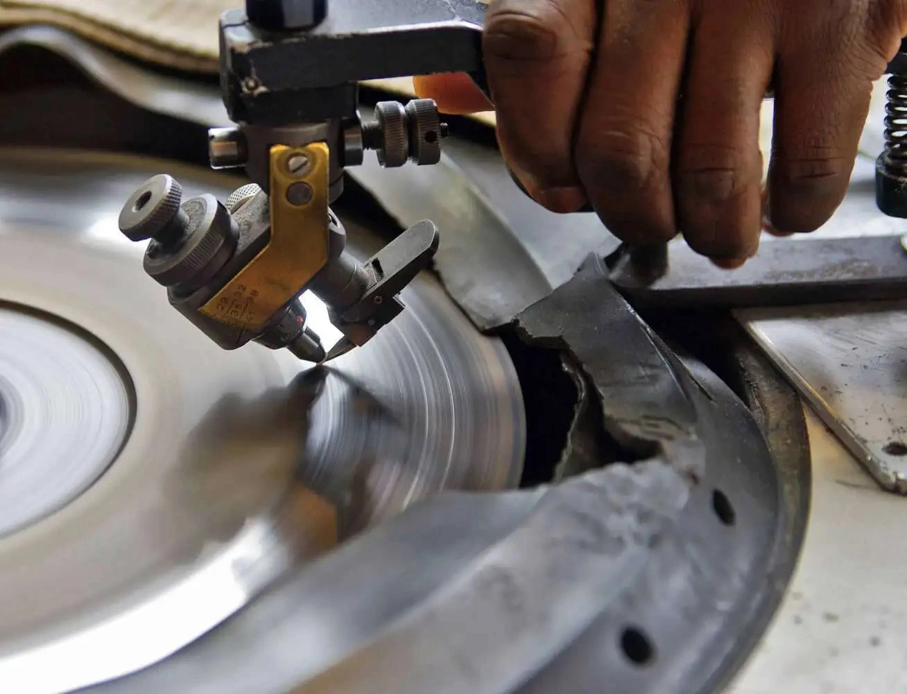
Post-slicing, the wafers are shaped and smoothed through peripheral grinding. This stage involves grinding the outer edge of the wafer to precise dimensions. Additionally, an orientation flat is added— a marked edge that indicates the crystallographic plane of the wafer, essential for later processing steps.
4. Double Disc Grinding or Lapping
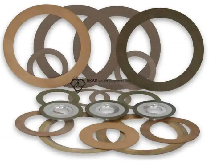
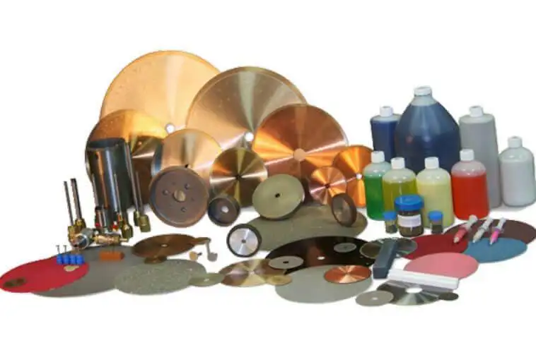
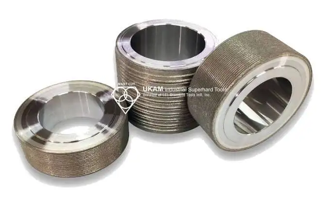
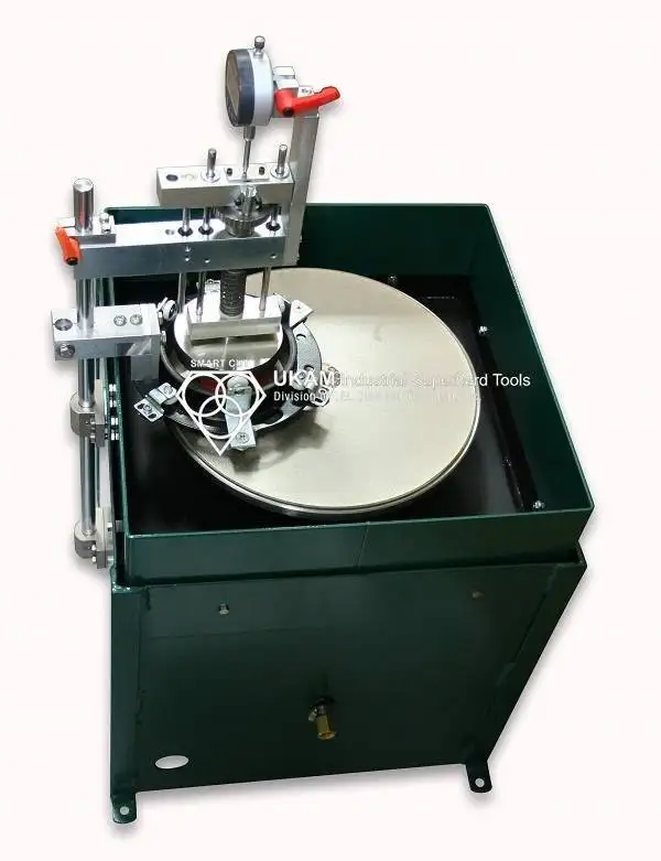
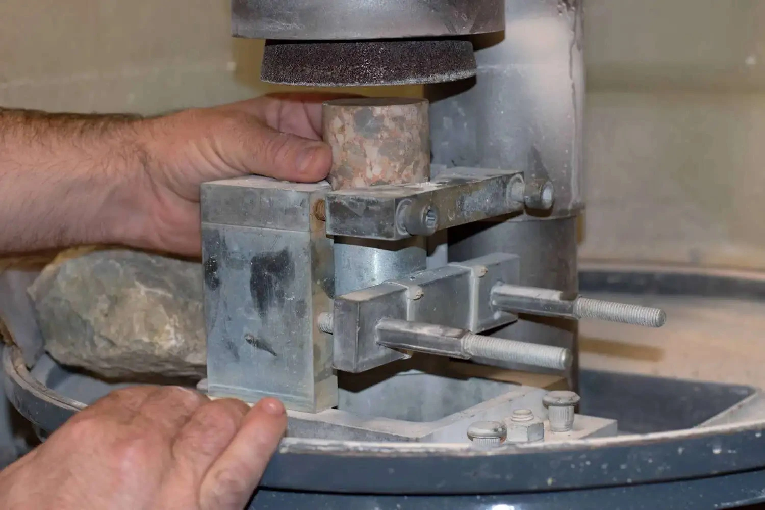
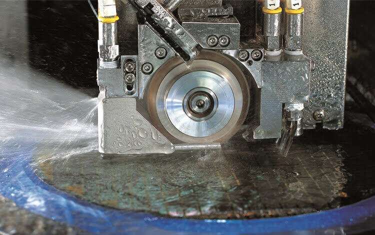
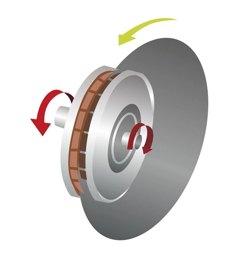
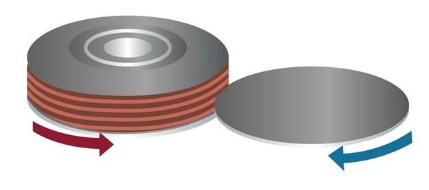
Double disc grinding or lapping is used to achieve parallelism and flatness on both sides of the silicon wafers simultaneously. In this process, two opposing grinding or lapping discs remove material from both faces of the wafer. This method is highly efficient for mass production as it allows high throughput with excellent control over thickness and flatness. Lapping, while similar to grinding, uses loose abrasive particles between the wafers and rotating discs, focusing on achieving a superior finish and removing any surface imperfections. More information on diamond double discs >>>
5. Ingot Slicing
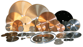
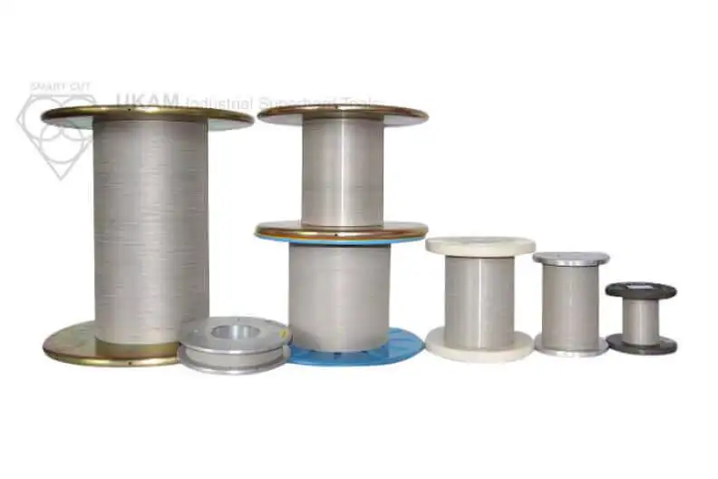
Slicing the ingot into individual silicon wafers is performed using precision tools such as ID (Inner Diameter) slicers using Inner Diameter Diamond Blades and diamond wire saws using diamond wire. These tools must offer exceptional precision to maintain the integrity and uniform thickness of the wafers, which are pivotal for the subsequent fabrication processes.
6. Surface and Edge Grinding
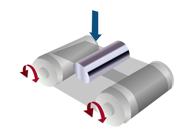
After shaping the periphery, the wafers undergo surface and edge grinding to achieve the required flatness and finish. This ensures that the wafers are perfectly flat and free from defects, which is vital for the uniformity of electronic circuits that will be built on them.
7. Back Grinding
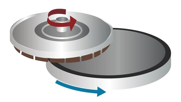
Back grinding refers to the process of thinning the silicon wafers after the circuits are constructed on the front side. This is done to reduce the wafer's thickness for better heat dissipation and flexibility in packaging. Find out more about diamond backgrinding wheels >>>
8. Chemical Mechanical Polishing (CMP)
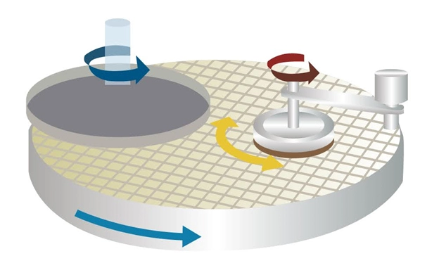
CMP is a hybrid technique that combines mechanical grinding and chemical etching to smooth the surface of the wafers to atomic-level flatness. This step is crucial as it prepares the wafer for the high-precision requirements of lithography, used in patterning the next layers.
9. Wafer Dicing
Once the wafers are processed and circuit patterns are created, they are diced into individual chips. This process uses precision dicing saws and blades to cut the wafer without damaging the circuits. The choice of blade, cutting speed, and coolant are carefully selected based on the material and circuit complexity. Find out more about dicing >>>
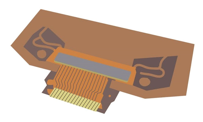
10. Molding and Packaging
The individual chips are then encapsulated in a protective molding compound that guards against physical damage and environmental factors. Following molding, the chips are packaged, which often involves connecting the silicon chip to its package leads with fine wires.
Final Inspection and Testing
The final stage involves thorough testing and inspection to ensure each chip meets the required specifications. Only after passing these tests are the chips deemed ready for integration into various electronic devices.
Ingot Production
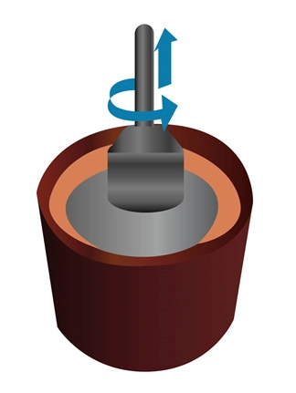
The production of silicon ingots marks the genesis of the semiconductor manufacturing process, setting the stage for the sophisticated electronics we rely on today. These ingots are typically created using the Czochralski (CZ) process, a method renowned for producing high-purity monocrystalline silicon. Here's how the process unfolds:
-
 1. Melting the Silicon: The process starts with pure silicon crystals, which are placed in a quartz crucible and heated to a high temperature until they melt. The purity of the silicon used here is crucial, as any impurities can affect the performance of the final semiconductor devices.
-
 2. Crystal Growth: A precisely oriented seed crystal is dipped into the molten silicon. The seed has the same lattice structure as the desired silicon crystal. As the seed is slowly withdrawn and rotated, the molten silicon crystallizes onto it, growing into a cylindrical ingot that maintains the seed’s crystal structure.
-
 3. Temperature Control: Throughout the growth process, the temperature of the molten silicon and the rate of pulling are meticulously controlled to ensure uniformity in the crystal structure, which is critical for the electrical properties of the semiconductor devices.
This method yields silicon with a uniform, defect-free crystal structure, which is ideal for the demanding requirements of semiconductor devices.
Ingot Cropping
After the ingot is grown, it undergoes cropping, which is the first of many precision steps in semiconductor fabrication. Cropping serves several essential functions:
-
 1. Removing the Seed and Tail: The initial and final parts of the ingot, where the seed was attached and where the crystal growth ended, are removed. These areas are likely to contain defects and impurities from the start and end of the growth process.
-
 2. Squaring the Ingot: The cylindrical ingot is often shaped into a more manageable form, such as a squared block, to optimize the slicing process. This squaring is achieved through precision cutting, where the outer edges of the cylindrical ingot are trimmed off.

-
 3. Quality Assurance: The cropped ingot is inspected for any macroscopic defects that might have occurred during growth. This includes checking for cracks, voids, or inclusions. Only ingots that meet stringent quality standards proceed to the next step of slicing.
-
 4. Preparation for Slicing: Cropping prepares the ingot for wafer slicing by ensuring the ends are flat and perpendicular to the axis of the ingot. This preparation is crucial for the subsequent slicing process, as it influences the thickness uniformity and surface quality of the wafers.
The quality of ingot production and cropping directly impacts the performance of the final semiconductor devices. Any imperfections introduced at this stage can propagate through later processes, resulting in flawed wafers that compromise the integrity of the circuits they host. Thus, the meticulous control of these early stages is paramount to the success of the entire semiconductor manufacturing process.
Commonly used tools include:
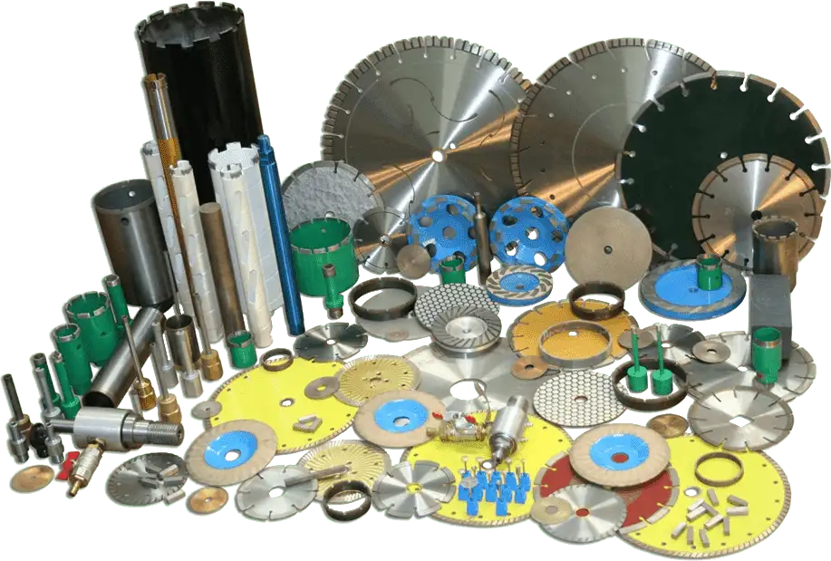
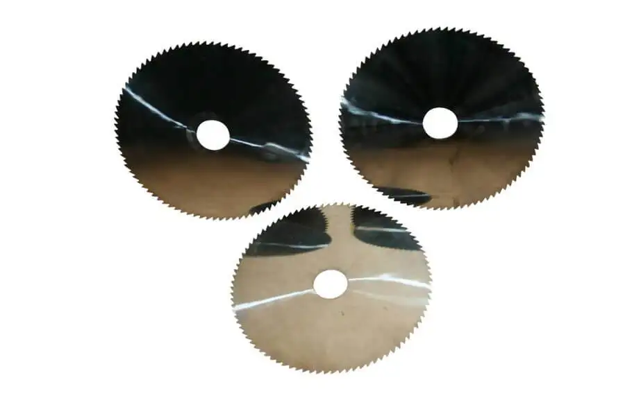
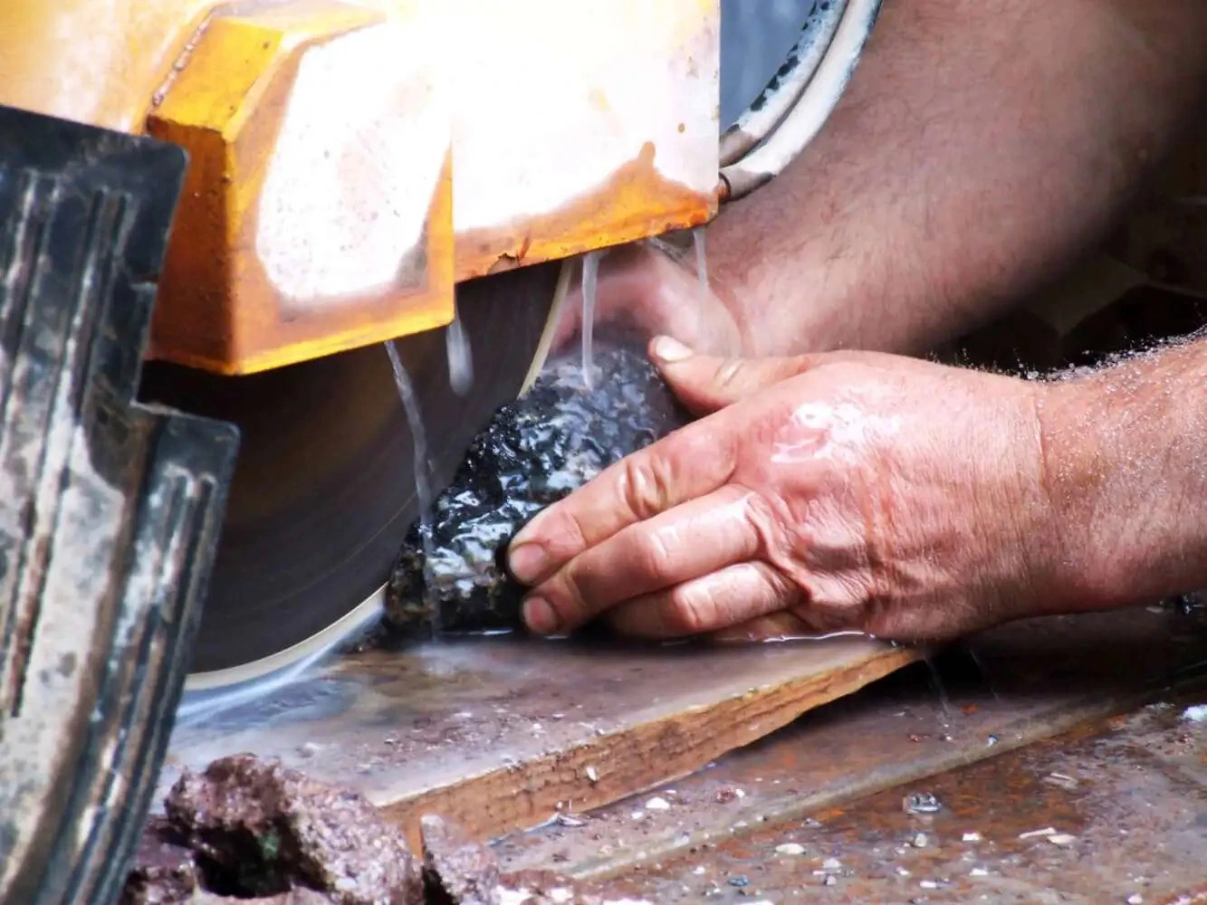
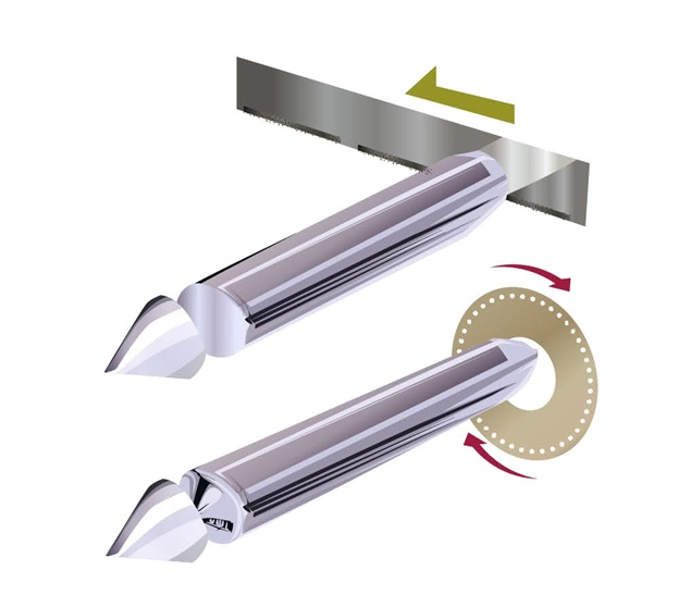
Diamond Saw Blades are extensively utilized for ingot cropping because they can cut through very hard materials like silicon, sapphire, and various metals and alloys. These blades are made from a metal alloy matrix embedded with diamond particles, which provide the necessary hardness and cutting capability. They are available in different grit sizes and concentrations to suit specific material hardness and cutting requirements and are designed to offer high precision, minimizing material loss and ensuring clean cuts.
Diamond Wire Saws are particularly useful for cutting very large or brittle ingots. They use a thin, tensioned wire coated with diamond or other abrasive materials and provide excellent precision and minimal material loss, making them ideal for materials like silicon and quartz.
ID cutting Blades - ID cutting blades are specialized tools designed for precision internal cutting of cylindrical materials such as tubes and pipes. These blades, often embedded with diamond or other abrasives, are small enough to fit inside the diameter they're cutting, making them ideal for precision engineering and aerospace applications where internal cuts must be accurate without altering the external surface.
Ingot Slicing
Ingot slicing is a critical process in semiconductor manufacturing, where large silicon ingots are cut into thin, flat wafers. This step requires extreme precision to ensure that the wafers are uniformly thick and free from defects, which is essential for the high-quality performance of semiconductor devices. The main tools used for this process are ID (Inner Diameter) slicers and diamond wire saws.
ID Slicers
ID slicers, or Inner Diameter slicers, utilize a thin, cylindrical blade with an abrasive edge, typically made from a hard material like diamond. The blade rotates at high speeds and is fed into the ingot, slicing it with precision. The key aspects of ID slicers include:
-
 1. Blade Quality: The quality of the blade is crucial as it needs to maintain its sharpness over many cuts to ensure consistent thickness across wafers.
-
 2. Cutting Technique: The ingot is slowly rotated while the blade cuts into it. This rotation helps achieve a uniform cut and minimizes the risk of chipping or cracking the silicon.
-
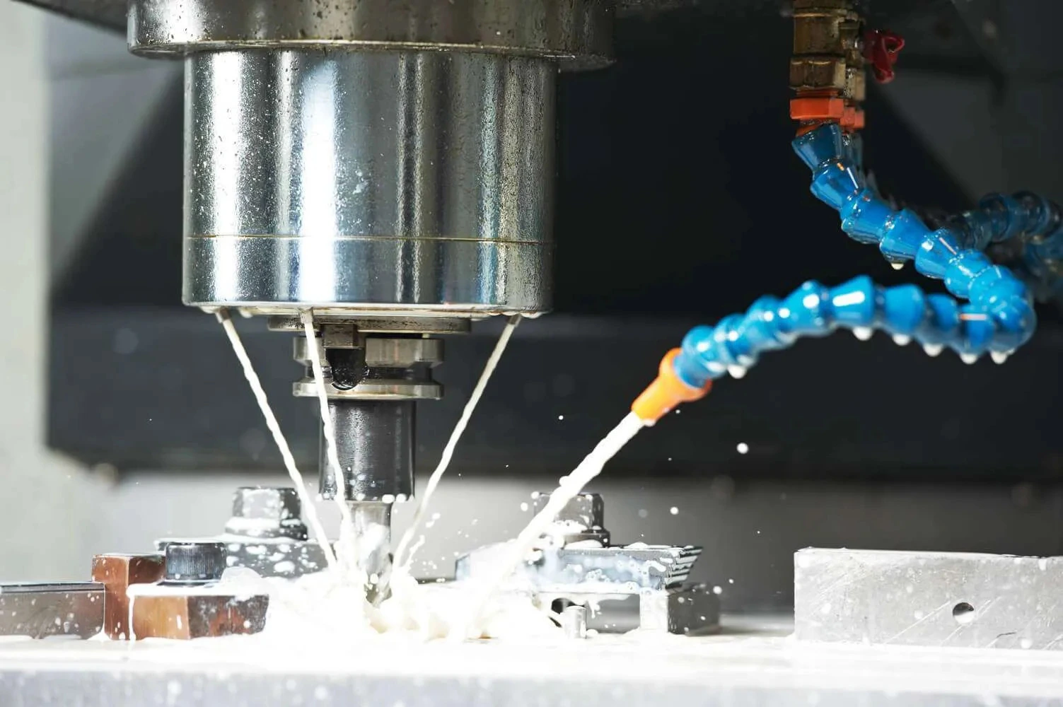
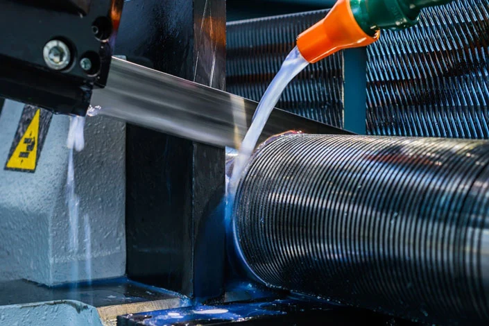
 3. Coolant Application: Coolants are used during slicing to prevent overheating, which can introduce defects into the silicon. Additionally, coolants help remove silicon particles that are generated during the cutting process.
Diamond Wire Saws
Diamond wire saws represent a more modern approach to slicing silicon ingots. These saws use a very thin wire embedded with diamond particles as the cutting edge. The advantages of diamond wire saws include:
-
 1. Thinner Wafers: Diamond wire saws can produce thinner wafers than traditional methods due to the smaller kerf (cut width) of the wire, which reduces material loss during slicing.
-
 2. Higher Efficiency: These saws can cut multiple wafers at once from a single ingot, significantly increasing throughput.
-
 3. Reduced Wafer Damage: The gentle cutting action of the diamond wire reduces mechanical stress on the wafers, thereby minimizing damage like cracks or warps.
The slicing process must be carefully controlled to ensure the quality of the wafers. Key considerations include:
-
 1. Speed and Feed Rate: The speed of the blade or wire and the feed rate of the ingot must be optimally adjusted to balance cutting efficiency with wafer quality.
-
 2. Wafer Thickness: The target thickness of the wafers depends on their final application. Precision in thickness is crucial because it influences the electrical properties of the wafers and the functionality of the finished semiconductor devices.
-
 3. Surface Smoothness: After slicing, the wafers often require additional surface treatment to achieve the necessary smoothness for photolithography, highlighting the importance of the initial slicing quality.
The precision with which wafers are sliced from the silicon ingot has a profound impact on the rest of the semiconductor manufacturing process. Any irregularities in thickness or surface quality can propagate errors through the subsequent photolithographic and doping processes, potentially leading to a higher rate of device failure. Therefore, ingot slicing is not just a matter of mechanical action but a finely tuned process that lays the groundwork for the high standards required in semiconductor production.
Peripheral Grinding and Orientation Flat
After the delicate process of slicing silicon ingots into thin wafers, the next critical step in semiconductor manufacturing is peripheral grinding. This procedure is essential for refining the shape and dimensions of the wafers, ensuring they meet stringent industry standards for subsequent processing steps.
Peripheral grinding focuses on the outer edge of the silicon wafer, serving multiple crucial purposes:
-
 1. Dimensional Accuracy: Ensures that the wafer's diameter and roundness adhere to precise specifications. This accuracy is vital for the wafers to fit correctly in the equipment used in later stages of semiconductor fabrication.
-
 2. Edge Quality: Improves the mechanical strength of the wafer by removing any microcracks and surface imperfections that could lead to breakage during processing. A smooth edge is less susceptible to chipping.
-
 3. Surface Preparation: Prepares the wafer for subsequent processing steps, such as layer deposition and photolithography, by ensuring a uniformly smooth edge that can influence the overall flatness and evenness of the wafer surface.
Peripheral grinding is performed using specialized grinding machines that are capable of achieving the necessary precision. These machines typically employ a rotating grinding wheel coated with an abrasive material such as diamond or silicon carbide. Key considerations in this process include:


-
 1. Grinding Wheel Speed: Must be carefully controlled to avoid excessive heat generation, which can damage the wafer.
-
 2. Feed Rate: The rate at which the wafer is fed into the grinding wheel affects both the finish quality and the rate of material removal.
-
 3. Coolant Application: Coolants are essential not only for temperature control but also for removing debris from the grinding area, thus preventing contamination and ensuring a clean cut.
Orientation Flat
An integral part of the wafer processing that occurs during the peripheral grinding stage is the creation of an orientation flat. This flat is a precisely ground edge on the wafer that serves several vital functions:
-
 1. Indicating Crystallographic Plane: The orientation flat marks the wafer's crystallographic plane, which is crucial for aligning the wafer correctly in subsequent processing equipment. Accurate alignment is essential for the photolithography steps, where patterns must be precisely positioned on the wafer.
-
 2. Handling and Identification: It also aids in the handling of wafers and helps operators and automated systems quickly identify the orientation and type of wafer, facilitating efficient and error-free processing.
-
 3. Standardization: The location and size of the orientation flat are standardized depending on the wafer diameter and type of silicon crystal (e.g., n-type or p-type), making it a universal marker used across the semiconductor industry.
The precision achieved during the peripheral grinding and the addition of an orientation flat are critical for the integrity and functionality of the final semiconductor devices. Any deviations in this stage can lead to alignment issues in layer deposition and patterning, which can ultimately affect the electrical properties and performance of the integrated circuits. Thus, maintaining high standards in this step is imperative for the production of reliable and efficient semiconductor devices.
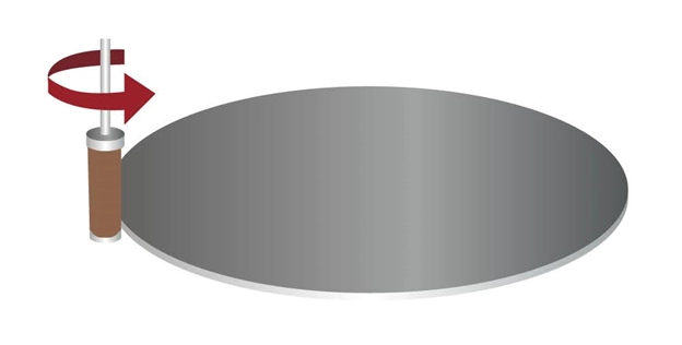
Surface and Edge Grinding
Once the peripheral dimensions of the silicon wafers are established through peripheral grinding, attention turns to surface and edge grinding. This stage is crucial for achieving the necessary flatness and surface quality for semiconductor fabrication, which involves intricate processes like photolithography and various deposition techniques.
Surface and edge grinding play several key roles. Firstly, surface grinding ensures the wafers are perfectly flat, which is vital for the success of subsequent photolithographic processes where any deviation can cause focus issues and pattern distortions. Secondly, edge grinding targets the wafer’s outer rim to remove microscopic cracks or chips that could propagate during processing and potentially lead to wafer breakage. Lastly, both grinding methods enhance the smoothness of the wafer's surface, essential for the uniform deposition of thin films and other materials in later stages.
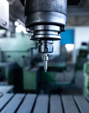
These grinding processes use specialized machines equipped with fine-grit, diamond-coated grinding wheels, performing under tightly controlled conditions. The selection of the grinding wheel is critical; wheels with finer abrasive particles are chosen for a smoother finish, while coarser grits are used for rapid material removal. Key grinding parameters such as wheel speed, feed rate, and depth of cut are carefully optimized to balance the removal rate with surface quality, and these parameters often vary depending on the type of silicon wafer and its intended application.
Coolants play an essential role in surface and edge grinding, minimizing thermal stress and flushing away silicon particles from the grinding interface. This prevents overheating and reduces the risk of surface contamination and damage.
Despite being routine, surface and edge grinding present several challenges. Maintaining uniform thickness across a single wafer and from one wafer to another is particularly challenging as wafer diameters increase. Grinding can also introduce sub-surface damage like micro-cracks and stresses, which must be minimized to ensure the mechanical and functional integrity of the wafers. Achieving the right balance in material removal is crucial; too much removal can weaken a wafer, while insufficient grinding may leave defects.


The quality of surface and edge grinding directly impacts the subsequent steps of semiconductor device fabrication. Imperfections in flatness or surface quality can adversely affect the lithography process, potentially leading to defective circuit patterns. Moreover, the integrity of the wafer's edges is critical to prevent breakage during handling, especially as wafers become larger and thinner.
Back Grinding
Back grinding is a crucial process in semiconductor manufacturing, aimed at thinning silicon wafers after circuits have been constructed on their front side. This step is essential for reducing the thickness of wafers, improving heat dissipation, and enhancing flexibility for various packaging applications, especially in high-performance electronics where efficient heat management and compact packaging are vital.
The process starts by mounting the wafers on a special adhesive film that secures them during grinding. This is crucial as it prevents any damage or breakage that could occur due to the thinning process. The primary tool used for back grinding is a grinding wheel made of a diamond-bonded matrix, which is capable of grinding silicon quickly and with precision. This grinding must be carefully controlled to reach the desired wafer thickness, often less than 100 microns for some applications.
During grinding, a cooling fluid is often used to prevent excessive heat build-up which could damage the wafer's surface and the underlying circuits. The fluid also assists in removing the silicon particles that are ground off. After grinding, the wafers may undergo a stress relief process, such as etching or applying a stress-relief layer, to remove any micro-cracks or surface stresses induced by the grinding.

One of the main challenges of back grinding is maintaining the integrity of the wafer surface. The process must be precise enough to thin the wafer without causing surface damage that could impair the functionality of the circuits. Handling and cleaning the wafers post-grinding are also critical, as any residual stress or particles left on the wafer can affect subsequent processes or the final performance of the semiconductor device. Additionally, the grinding process can introduce sub-surface damage, such as micro-cracks and dislocations, which might not be visible but can affect the reliability and performance of the semiconductor devices. To address these issues, advanced techniques like dry polishing or chemical mechanical polishing (CMP) are often employed after back grinding to remove or reduce such damage.
Recent advancements in back grinding technology include the development of more precise grinding equipment and techniques that can achieve thinner wafer specifications without compromising the wafer's structural integrity. Innovations such as ultra-fine grinding wheels and laser-assisted grinding have been explored to enhance the quality and efficiency of the back grinding process.
Chemical Mechanical Polishing (CMP)
Chemical Mechanical Polishing (CMP) is a critical technique used extensively in the semiconductor industry to achieve ultra-smooth surfaces on silicon wafers, essential for the high-performance requirements of modern electronic devices. CMP combines mechanical abrasion with chemical etching to efficiently and precisely polish wafer surfaces, removing microscopic defects and achieving high levels of planarity. This process is crucial for the fabrication of integrated circuits and microchips, where even minor surface irregularities can lead to significant performance issues.
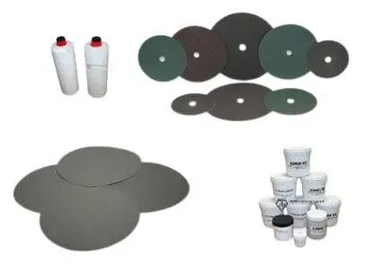
CMP involves using a chemically active slurry and a polishing pad to remove material from the wafer's surface. The slurry typically contains abrasive particles like silica or cerium oxide, suspended in a chemically reactive solution. The chemicals in the slurry interact with the silicon surface, softening it and making it more susceptible to removal by the mechanical action of the abrasive particles. The chemical action involves the slurry’s reactive agents etching the silicon surface, selectively weakening the top atomic layers. Concurrently, the mechanical action involves the physical abrasion by the rotating pad, which applies controlled pressure and motion to remove the softened material.
The polishing pad, a critical component in CMP, is typically made from polyurethane or other soft materials, which contour to the wafer's surface. These pads must be periodically conditioned to maintain their effectiveness and ensure uniform application of pressure across the wafer.

The composition of the slurry is tailored to the specific material being polished and the desired outcome, with particle size, concentration, and chemical properties optimized to achieve the best balance between chemical etching and mechanical abrasion.
Several parameters are crucial in optimizing CMP performance, including the downward pressure exerted on the wafer, the relative speed at which the pad and the wafer move, and the environment's temperature. These factors affect the rate of material removal, the quality of the polish, and the chemical reactions involved in the process.
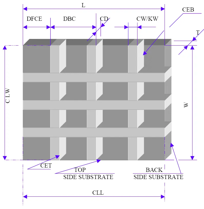
CMP must address several challenges, such as controlling the uniformity of material removal across the wafer, preventing the introduction of new defects during polishing, and managing the environmental impact of spent slurry. Innovations in pad technology, slurry composition, and machine design continually improve the efficiency and effectiveness of CMP. For instance, advancements in slurry formulations aim to reduce particle size for finer polishing, while improvements in pad design focus on enhancing pad life and the consistency of wafer-to-pad contact.
Wafer Dicing
Wafer dicing is the final step in the semiconductor manufacturing process, where processed wafers with circuit patterns are cut into individual chips or die. This crucial phase involves using precision dicing saws and blades to separate the individual circuits into discrete units that can be packaged and used in electronic devices. The entire process must be conducted with precision and care to avoid damaging the delicate circuits on the wafers.
The most common tool for wafer dicing is the dicing saw, which employs a high-speed rotating blade made typically of diamond or another hard material capable of cutting through silicon and other semiconductor materials. The choice of blade is critical and is based on the wafer material, the size of the die, and the complexity of the circuitry. Thinner blades are preferred to minimize material loss due to the width of the cut, known as the kerf, which is particularly important when working with small or densely packed circuits.
The speed of the blade's movement through the wafer also requires careful adjustment. Faster speeds can lead to quicker operations but might increase the risk of generating excessive heat or causing chips and cracks. Coolants are essential during the dicing process to mitigate heat build-up and to remove debris from the cutting area, helping to protect the circuits by reducing thermal stress and preventing contamination.
Before dicing, wafers are mounted on a sticky film to keep them stable and to ensure that the cut pieces remain in place. The mounting process must avoid introducing bubbles or other defects that could affect cutting accuracy. In some cases, particularly for brittle or mechanically sensitive materials, a scribing technique is used before the actual separation. Scribing involves creating a shallow cut or a perforated line on the wafer, facilitating a cleaner break along precise lines without applying mechanical force.
The biggest challenges in wafer dicing include minimizing damage such as chipping, cracking, or contamination, which can impair chip functionality. Material loss during dicing can be significant, especially for valuable materials or when the kerf width is large, necessitating optimization of blade thickness and cutting parameters. Additionally, balancing speed and precision is crucial as higher throughput (faster dicing processes) can sometimes compromise the quality of the dice.


