


-
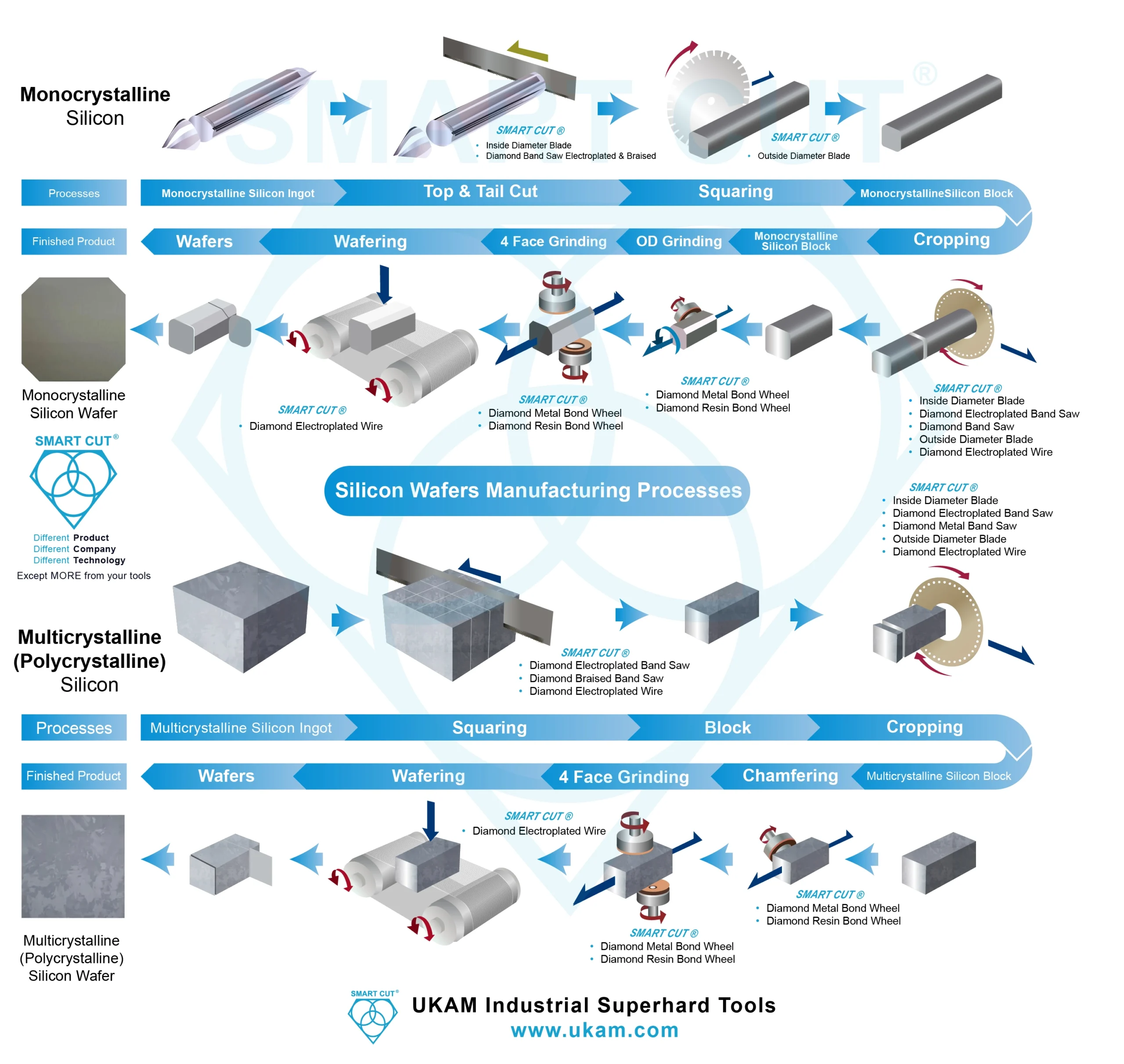
 1. Melting the Silicon: The process starts with pure silicon crystals, which are placed in a quartz crucible and heated to a high temperature until they melt. The purity of the silicon used here is crucial, as any impurities can affect the performance of the final semiconductor devices.
 -
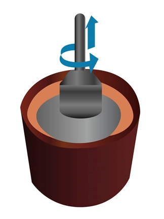
2. Crystal Growth: A precisely oriented seed crystal is dipped into the molten silicon. The seed has the same lattice structure as the desired silicon crystal. As the seed is slowly withdrawn and rotated, the molten silicon crystallizes onto it, growing into a cylindrical ingot that maintains the seed’s crystal structure.
-
3. Temperature Control: Throughout the growth process, the temperature of the molten silicon and the rate of pulling are meticulously controlled to ensure uniformity in the crystal structure, which is critical for the electrical properties of the semiconductor devices.
-
1. Removing the Seed and Tail: The initial and final parts of the ingot, where the seed was attached and where the crystal growth ended, are removed. These areas are likely to contain defects and impurities from the start and end of the growth process.
-
2. Squaring the Ingot: The cylindrical ingot is often shaped into a more manageable form, such as a squared block, to optimize the slicing process. This squaring is achieved through precision cutting, where the outer edges of the cylindrical ingot are trimmed off.
-
3. Quality Assurance: The cropped ingot is inspected for any macroscopic defects that might have occurred during growth. This includes checking for cracks, voids, or inclusions. Only ingots that meet stringent quality standards proceed to the next step of slicing.
-
4. Preparation for Slicing: Cropping prepares the ingot for wafer slicing by ensuring the ends are flat and perpendicular to the axis of the ingot. This preparation is crucial for the subsequent slicing process, as it influences the thickness uniformity and surface quality of the wafers.
-
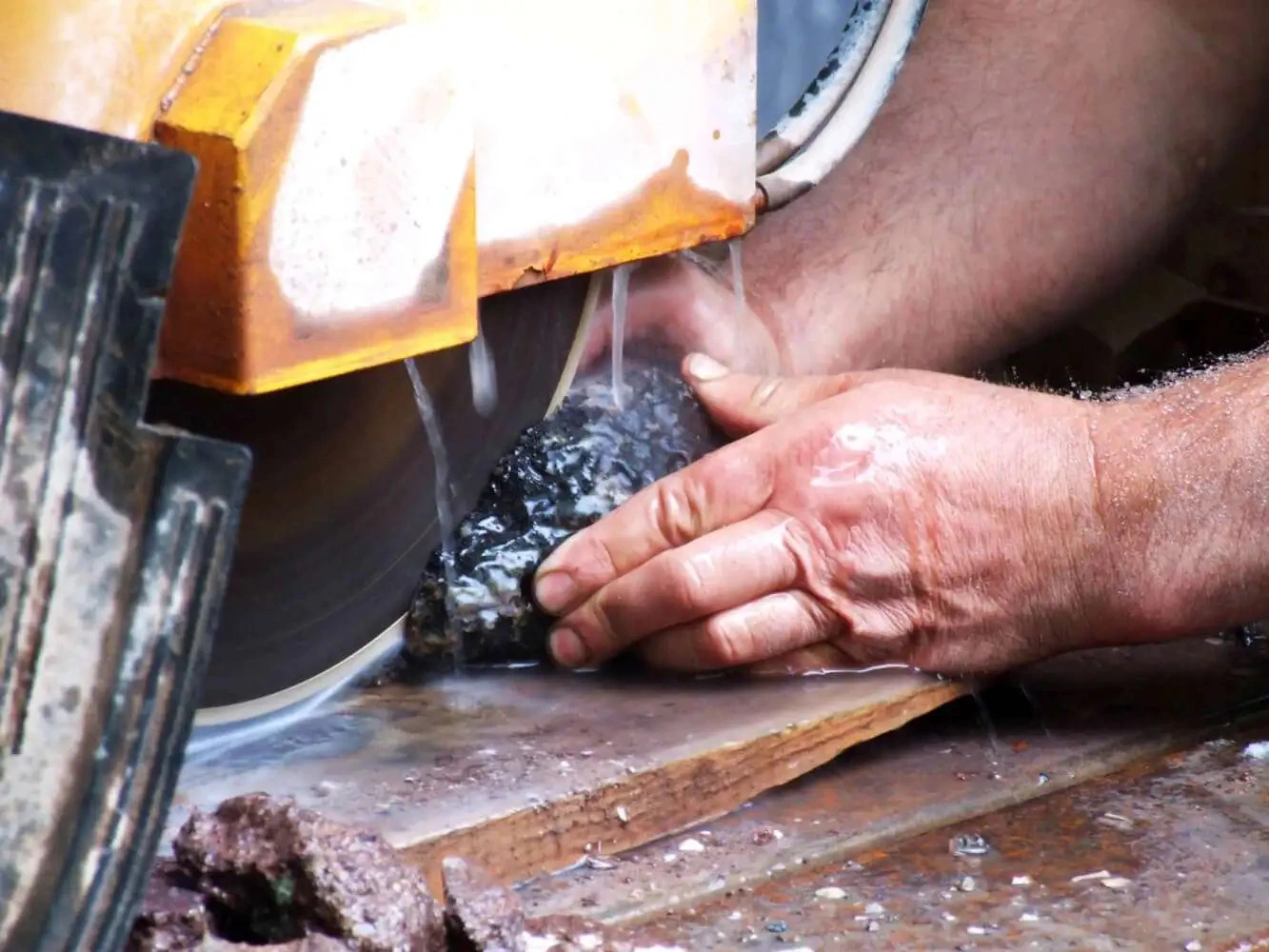
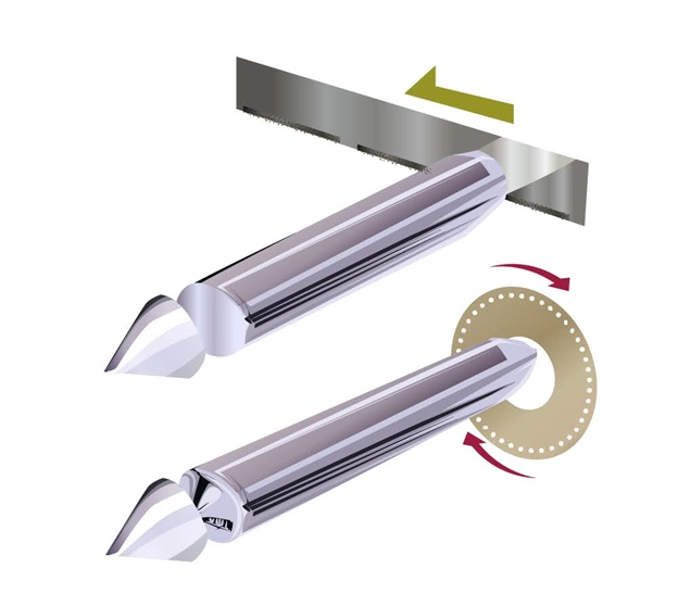
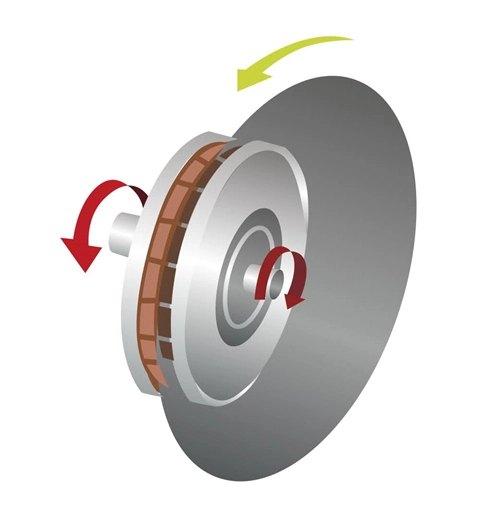
1. Blade Quality: The quality of the blade is crucial as it needs to maintain its sharpness over many cuts to ensure consistent thickness across wafers.
-
2. Cutting Technique: The ingot is slowly rotated while the blade cuts into it. This rotation helps achieve a uniform cut and minimizes the risk of chipping or cracking the silicon.
-
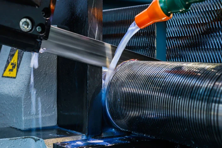
3. Coolant Application: Coolants are used during slicing to prevent overheating, which can introduce defects into the silicon. Additionally, coolants help remove silicon particles that are generated during the cutting process.
-
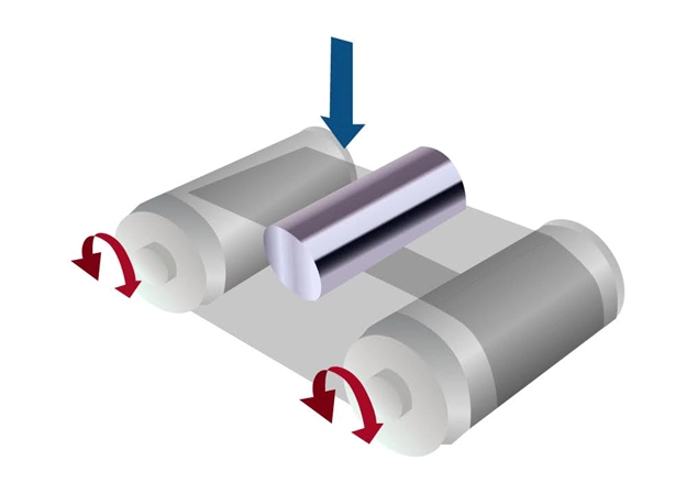
1. Thinner Wafers: Diamond wire saws can produce thinner wafers than traditional methods due to the smaller kerf (cut width) of the wire, which reduces material loss during slicing.
-
2. Higher Efficiency: These saws can cut multiple wafers at once from a single ingot, significantly increasing throughput.
-
3. Reduced Wafer Damage: The gentle cutting action of the diamond wire reduces mechanical stress on the wafers, thereby minimizing damage like cracks or warps.
-
1. Speed and Feed Rate: The speed of the blade or wire and the feed rate of the ingot must be optimally adjusted to balance cutting efficiency with wafer quality.
-
2. Wafer Thickness: The target thickness of the wafers depends on their final application. Precision in thickness is crucial because it influences the electrical properties of the wafers and the functionality of the finished semiconductor devices.
-
3. Surface Smoothness: After slicing, the wafers often require additional surface treatment to achieve the necessary smoothness for photolithography, highlighting the importance of the initial slicing quality.
-
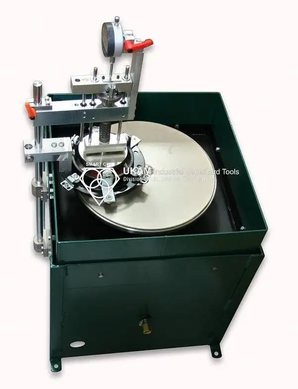
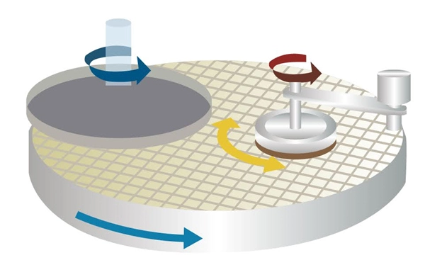
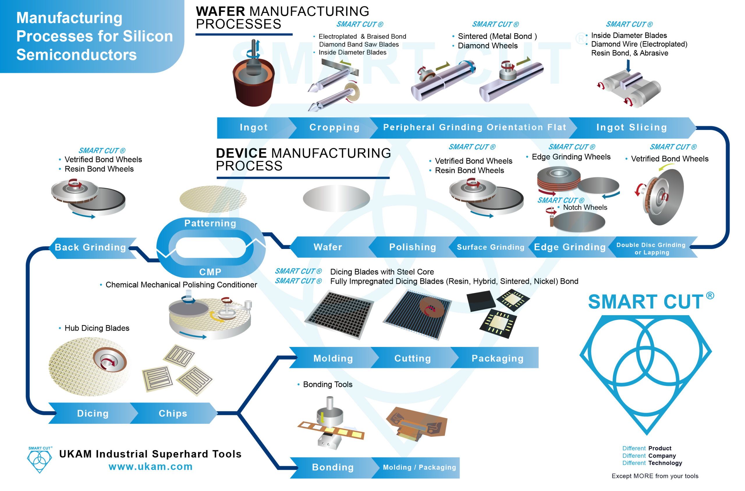
1. Dimensional Accuracy: Ensures that the wafer's diameter and roundness adhere to precise specifications. This accuracy is vital for the wafers to fit correctly in the equipment used in later stages of semiconductor fabrication.
-
2. Edge Quality: Improves the mechanical strength of the wafer by removing any microcracks and surface imperfections that could lead to breakage during processing. A smooth edge is less susceptible to chipping.
-
3. Surface Preparation: Prepares the wafer for subsequent processing steps, such as layer deposition and photolithography, by ensuring a uniformly smooth edge that can influence the overall flatness and evenness of the wafer surface.
-
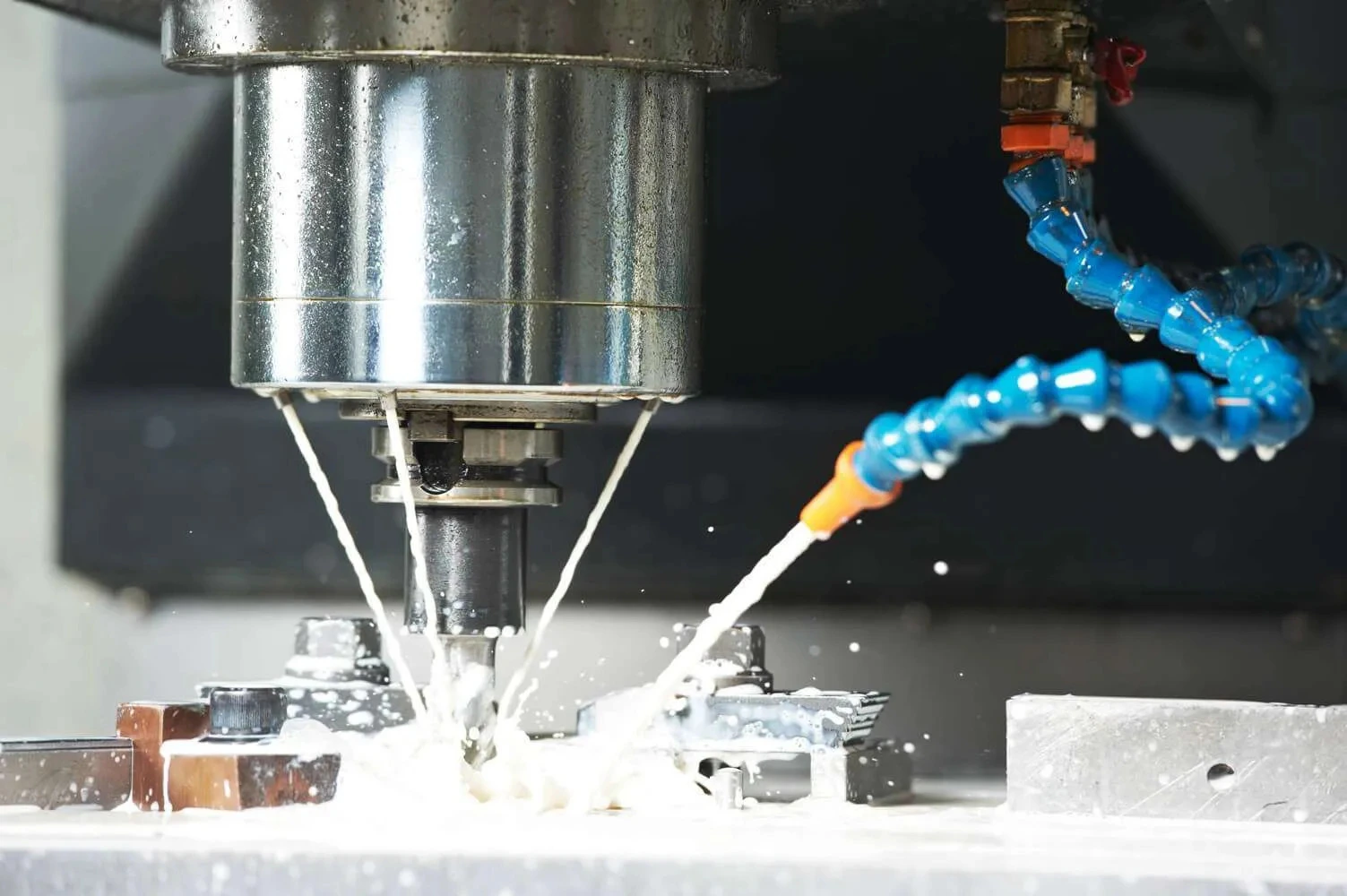
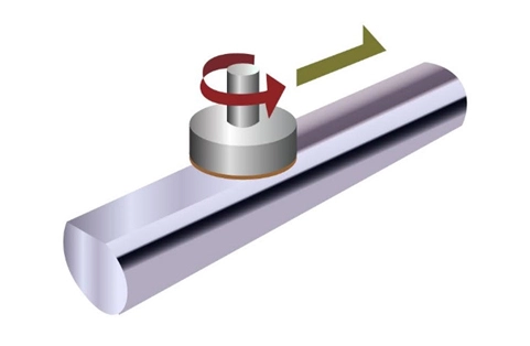
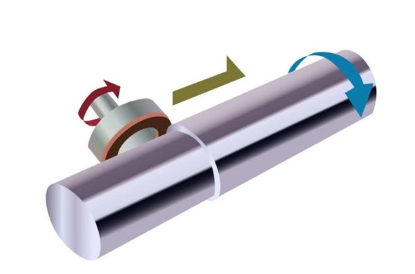
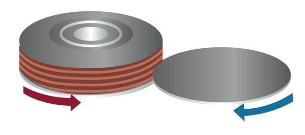
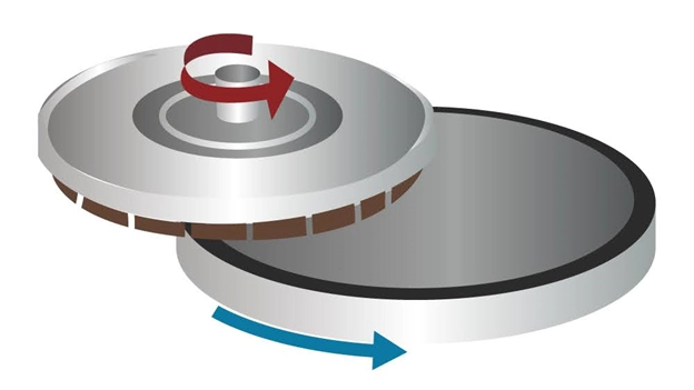
1. Grinding Wheel Speed: Must be carefully controlled to avoid excessive heat generation, which can damage the wafer.
-
2. Feed Rate: The rate at which the wafer is fed into the grinding wheel affects both the finish quality and the rate of material removal.
-
3. Coolant Application: Coolants are essential not only for temperature control but also for removing debris from the grinding area, thus preventing contamination and ensuring a clean cut.
-
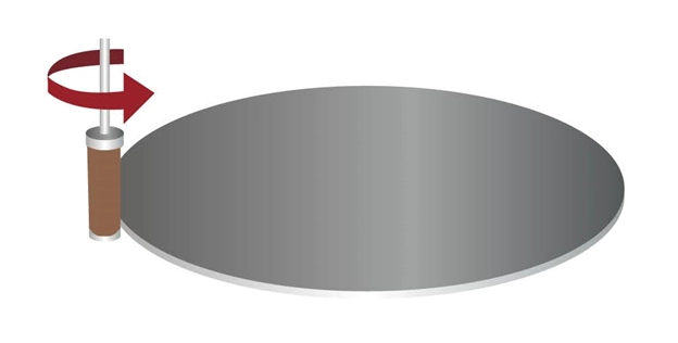
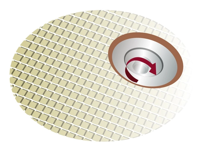
1. Indicating Crystallographic Plane: The orientation flat marks the wafer's crystallographic plane, which is crucial for aligning the wafer correctly in subsequent processing equipment. Accurate alignment is essential for the photolithography steps, where patterns must be precisely positioned on the wafer.
-
2. Handling and Identification: It also aids in the handling of wafers and helps operators and automated systems quickly identify the orientation and type of wafer, facilitating efficient and error-free processing.
-
3. Standardization: The location and size of the orientation flat are standardized depending on the wafer diameter and type of silicon crystal (e.g., n-type or p-type), making it a universal marker used across the semiconductor industry.

Alexander Schneider is a senior applications engineer with over 35 years of hands on experience in industrial diamond tooling. He specializes in the development, application, and optimization of ultra-thin and high-precision diamond blades, diamond core drills, and diamond and CBN grinding wheels for advanced materials.
His work spans ceramics, glass, composites, semiconductors, and high-performance metals. He supports research laboratories and manufacturing environments by optimizing tool design and cutting parameters to achieve high cut quality, long tool life, material integrity, and consistent process results.

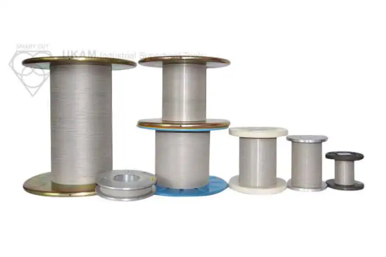
Guide to Diamond Wire Sawing: Technologies, Wire Types, and Machine Designs
Selecting the Right Diamond Band Saw blade for your Application
Diamond Band Saw Blades Usage Recommendations & Best Practices

Diamond Wire vs band saw blades and circular blades
The Comprehensive Guide to the Processes of Silicon Wafers Production
Manufacturing Processes for Silicon Semiconductors From Ingot to Integrated Circuit
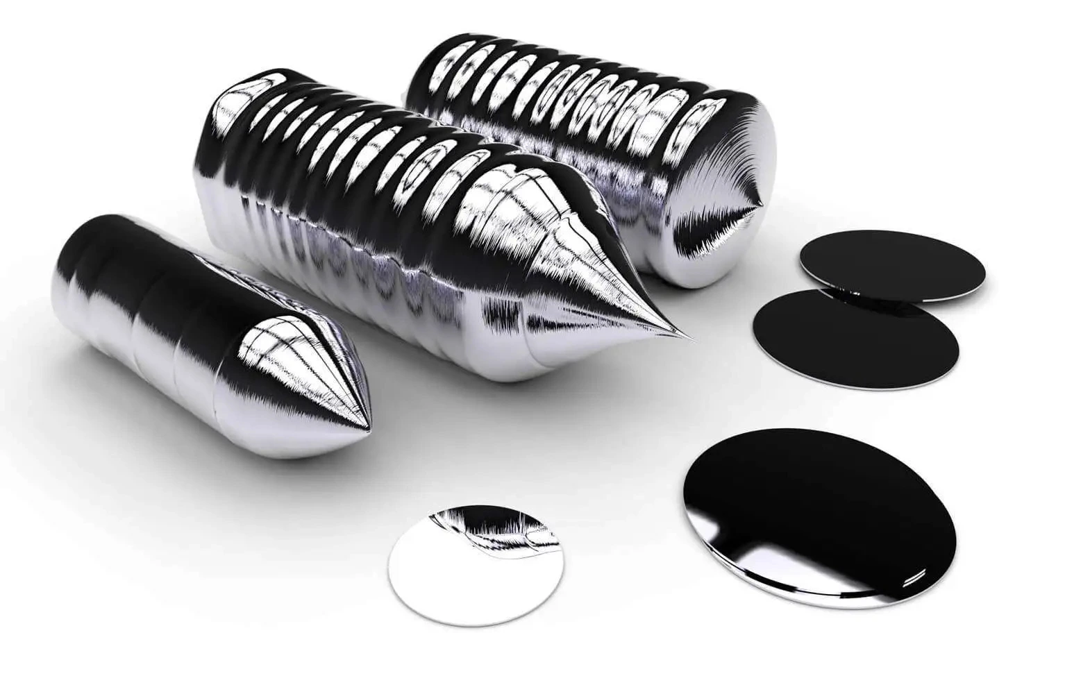
1. Ingot Production The journey begins with the creation of silicon ingots, which are pure silicon cylinders produced through methods like the Czochralski process. Once formed, these ingots undergo a cropping procedure to remove any excess and to prepare them for slicing. This step ensures that only the highest quality silicon is used, which is crucial for the performance of the final semiconductor devices.

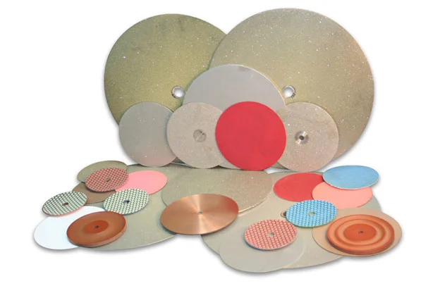
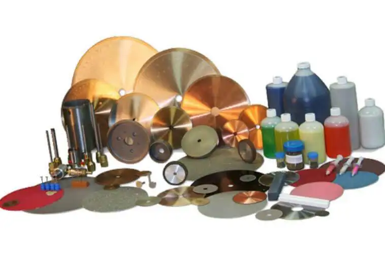
Evaluating & Comparing Diamond Blades
Proper testing procedures and methodologies must be set up and used to obtain accurate as well as repeatable testing results. This article will discuss several simple procedures which have been used under actual field conditions, verifying their feasibility for testing diamond cut off wheels.

How to Improve & Optimize Your Diamond Sawing Operation

Troubleshooting Diamond Sawing Problems

Silicon Fabrication Guide

Why use diamond
Diamond is the hardest material known to man kind. When used on diamond/tools, diamond grinds away material on micro (nano) level. Due to its hardness Diamond will work all types of materials from hardness of 40 on Rockwell scale and up. Diamond will machine hardest material, including those materials that other conventional types of abrasives, carbide and high speed steel will not.

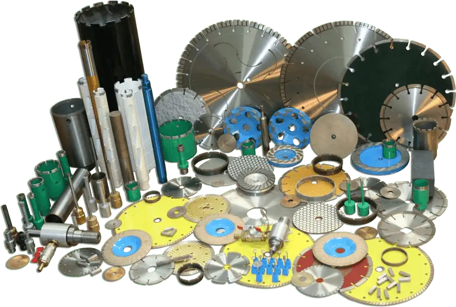
How to Selecting Right Diamond Tools for your application
Alexander Schneider is a senior applications engineer with over 35 years of hands on experience in industrial diamond tooling. He specializes in the development, application, and optimization of ultra-thin and high-precision diamond blades, diamond core drills, and diamond and CBN grinding wheels for advanced materials.
His work spans ceramics, glass, composites, semiconductors, and high-performance metals. He supports research laboratories and manufacturing environments by optimizing tool design and cutting parameters to achieve high cut quality, long tool life, material integrity, and consistent process results.