


-
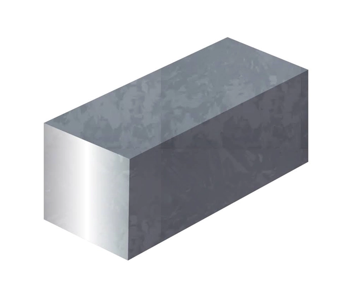
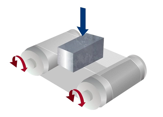
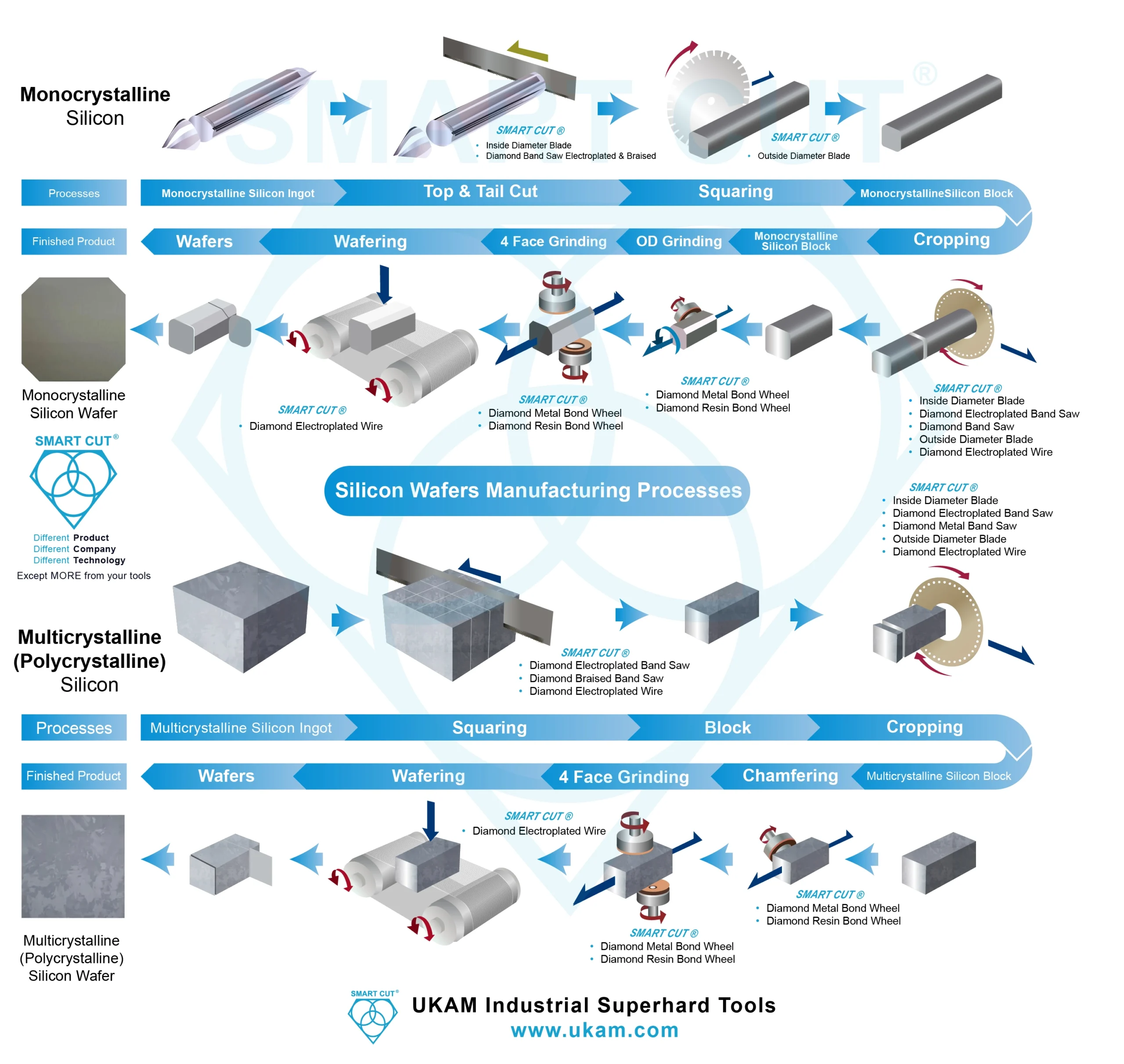
 Uniformity and Consistency: Squared ingots ensure that wafers are produced with consistent dimensions and properties, which is critical for the high standards required in semiconductor manufacturing and photovoltaic applications.
 -
Optimal Use of Material: By converting the cylindrical ingot into a squared shape, manufacturers can maximize the use of the material, reducing waste and improving the yield of valuable wafers.
-
Enhanced Handling and Mounting: Squared ingots are easier to handle, align, and mount on slicing equipment, which reduces the risk of errors during the cutting process.
-
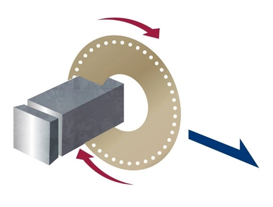
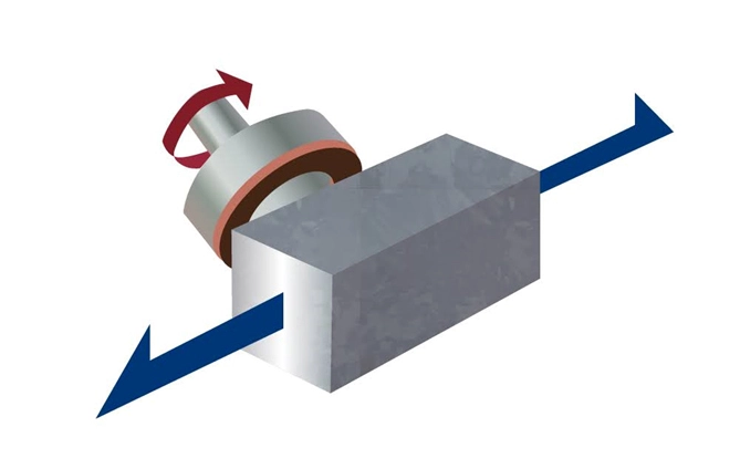
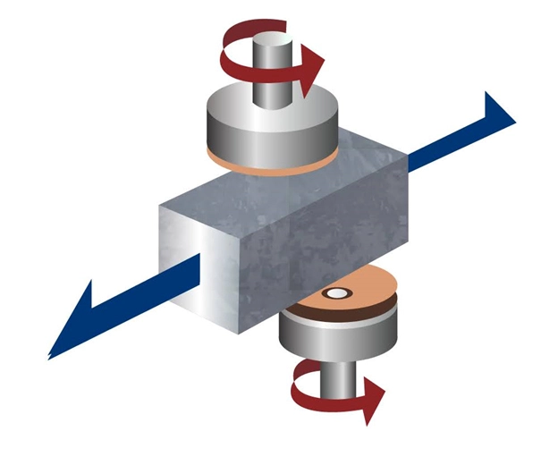
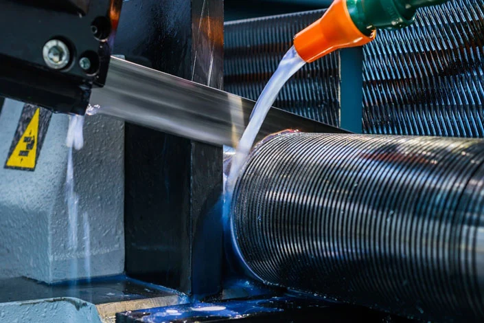
Speed of the wire: Adjusting the speed can help control the rate of cutting and reduce thermal damage to the wafers.
-
Tension on the wire: Proper tension ensures that the wire does not sag or break, which can affect the consistency of the cut.
-
Coolant flow: The use of coolants not only reduces the heat generated during cutting but also helps in flushing away any debris, which could otherwise scratch the wafer surface.
-
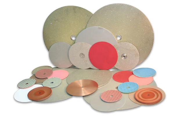
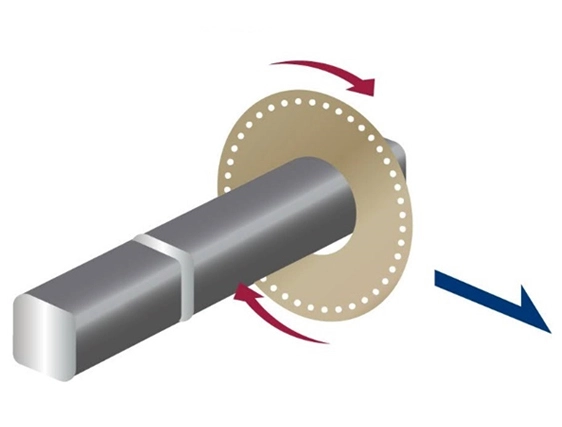
1. Mechanical Grinding: This is the most common method, where mechanical grinders equipped with diamond-tipped wheels are used to shave off the sharp edges of the wafers. This method is highly effective and can be adjusted for different chamfer sizes.
-
2. Laser Chamfering: For applications requiring high precision and minimal physical contact, laser chamfering can be used. This method involves using a focused laser beam to melt and reshape the wafer’s edge. It's particularly useful for very thin or delicate wafers where mechanical stress needs to be minimized.
-
3. Chemical Etching: In some cases, chemical etching processes are used to chamfer the edges. This involves exposing the wafer edges to chemical agents that selectively remove material, rounding off the edges. This method is less common but can be advantageous for certain types of semiconductor materials.
-
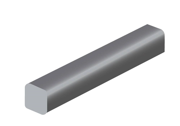
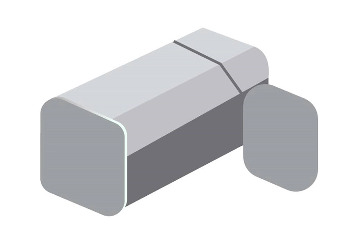
Enhanced Material Utilization: By transforming the ingot into a squared block, the process significantly reduces silicon wastage. The uniform shape allows for more efficient layout and cutting patterns when the wafers are subsequently sliced, maximizing the number of wafers obtained per ingot.
-
Improved Processing Efficiency: Squared ingots can be easily stacked, stored, and transported, reducing logistical challenges. Additionally, their uniform shape facilitates automated processing in later stages, enhancing the overall efficiency of the wafer production line.
-
Quality Consistency: While multicrystalline silicon does not possess the same level of crystallographic uniformity as monocrystalline silicon, squaring helps in maintaining as much consistency as possible. A uniform block ensures consistent heat distribution during subsequent thermal processes, which is vital for maintaining quality across the batch.
-
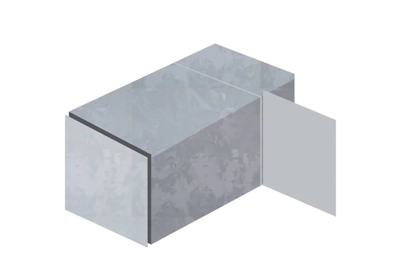
Standardization of Raw Material: By cutting the ingot into uniform blocks, manufacturers can standardize the starting material for the wafering process. This standardization is critical for automated mass production, allowing for consistent settings on machines in the cropping and wafering stages.
-
Optimized Material Use: Block formation is strategically planned to maximize the yield from each ingot. The dimensions of each block are calculated to minimize waste during the wafering process, thereby enhancing the overall efficiency of silicon utilization.
-
Improved Handling and Processing: Smaller blocks are easier to handle and process than large ingots. This ease of handling reduces the risk of damage during transport and processing, which is crucial for maintaining the integrity of the silicon, a material that is inherently brittle and prone to cracking under stress.
-
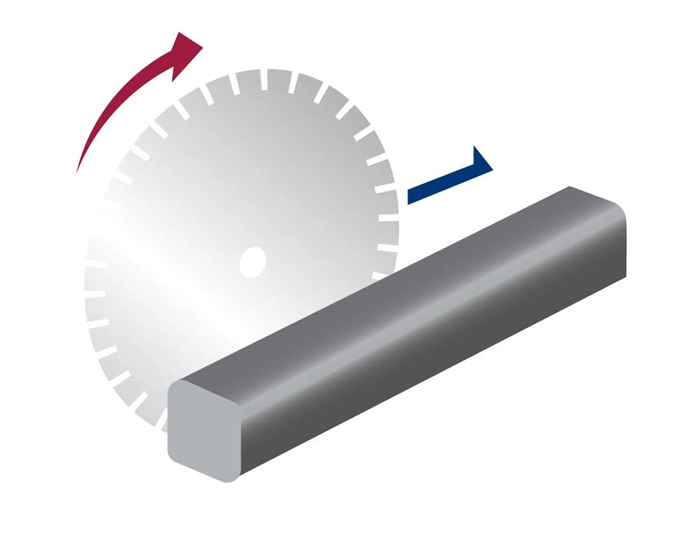
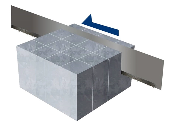
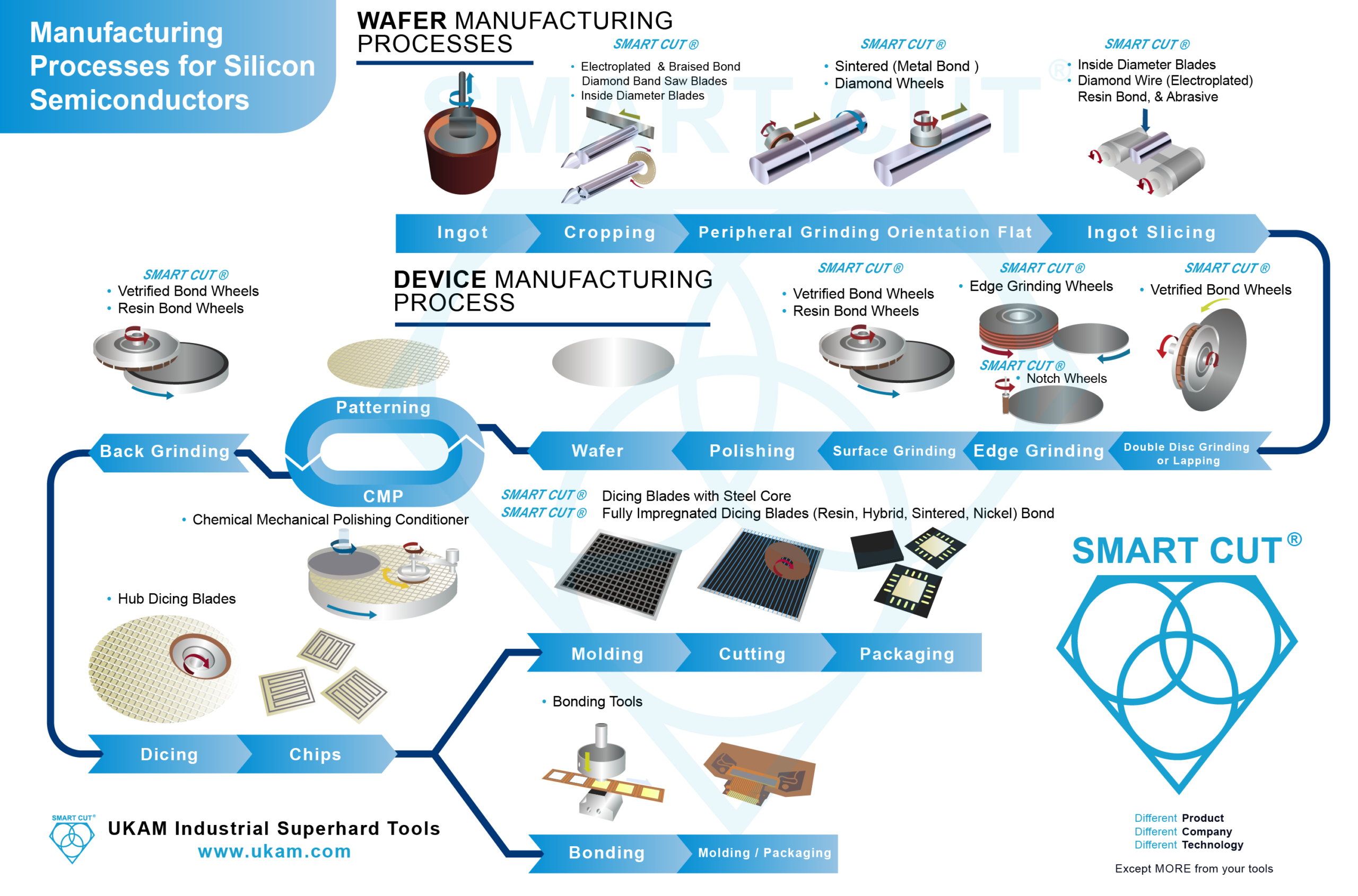
Uniformity and Precision: By ensuring that each piece is cut to precise specifications, cropping aids in the uniformity of the wafers produced. Uniform wafers are crucial for the semiconductor industry, where variations in thickness or flatness can lead to significant performance issues in electronic devices.
-
Material Efficiency: Cropping is designed to maximize the number of viable wafers that can be produced from each block. By optimizing the dimensions of each cropped piece, manufacturers can reduce waste and increase the overall yield of the production process.
-
Process Consistency: Consistent cropping practices help standardize the subsequent processing stages, including polishing and etching, ensuring that these processes can be conducted under uniform conditions to produce high-quality wafers.
-
Control of Defects: The cropping process must be carefully controlled to avoid introducing defects such as cracks, chips, or microfractures into the silicon. Such defects can undermine the structural integrity of the wafers and render them unsuitable for high-precision applications.
-
Dimensional Accuracy: Maintaining dimensional accuracy is crucial, as any deviations can affect the alignment and layering processes in semiconductor manufacturing, potentially leading to defective electronic components.
-
Equipment Precision: The precision of the cropping equipment is fundamental. Wear and tear on blades or wires can lead to inconsistent cuts. Regular maintenance and calibration of equipment are necessary to ensure ongoing accuracy and efficiency.
-
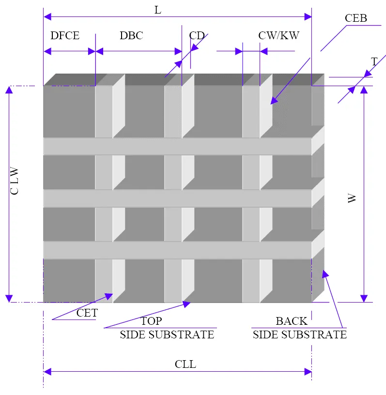
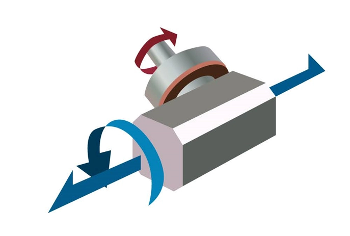
Thickness Control: One of the primary goals of OD grinding is to achieve uniform wafer thickness. Uniform thickness is critical for processes like photolithography and etching, where depth precision is necessary for pattern accuracy and functionality of semiconductor circuits.
-
Improved Surface Quality: OD grinding helps in achieving a mirror-like surface finish that is essential for high-performance semiconductor applications. A smoother surface reduces scattering of light and electrons, which is crucial for the efficient function of devices like sensors and optical components.
-
Edge Integrity: The process also involves ensuring that the edges of the wafers are smooth and free from defects. Properly ground edges reduce the risk of chipping and cracking during handling and processing, thereby increasing the yield of usable wafers.
-
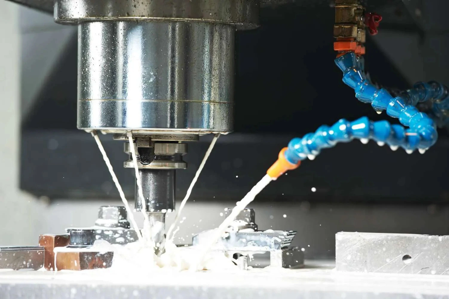
Thermal Damage: The grinding process generates significant heat, which can affect the structural integrity of the silicon if not properly managed. Effective cooling systems are essential to dissipate heat and prevent thermal damage, such as slip dislocations or warping.
-
Material Removal Rate: Balancing the rate of material removal is critical. Removing too much material too quickly can lead to defects, while too slow a rate can be inefficient and economically non-viable.
-
Equipment Precision: The precision of the grinding equipment is vital. Wear and tear on the grinding wheels or belts can lead to inconsistencies in wafer thickness or surface finish. Regular maintenance and calibration of equipment are necessary to ensure ongoing accuracy.
-
Increased Handling Safety: Chamfered edges make the wafers safer to handle. This is crucial in environments where manual handling of wafers is necessary, as it minimizes the risk of injury to personnel from sharp edges.
-
Enhanced Durability: By smoothing the wafer edges, chamfering reduces the likelihood of edge defects that can propagate into larger cracks during high-temperature processes such as oxidation and deposition.
-
Improved Process Integration: Many semiconductor manufacturing processes, such as lithography and etching, require precise alignment and uniform exposure. Chamfered edges contribute to better alignment and loading of wafers into process equipment, ensuring consistent processing across the entire wafer surface.
-
Mechanical Grinding: This is the most commonly used method for chamfering, where grinding wheels or belts are used to bevel the wafer edges. This technique is appreciated for its speed and ability to handle large batches of wafers.
-
Laser Chamfering: For high precision requirements, laser chamfering offers a contactless method to achieve a clean and controlled edge profile. This method is particularly useful for very thin or fragile wafers where mechanical stress needs to be minimized.
-
Chemical Etching: Chamfering can also be performed using chemical etching techniques, which remove material from the wafer edges by chemical action. This method is less common but can be advantageous for certain material types or when a very specific edge profile is required.
-
Process Control: The chamfering process parameters such as speed, pressure, and temperature must be meticulously managed to ensure consistent edge quality across all wafers.
-
Material Removal Accuracy: Excessive material removal can weaken the wafer's structural integrity, while insufficient chamfering might not effectively reduce the risk of edge damage.
-
Integration with Other Processes: Chamfering must be seamlessly integrated into the wafer fabrication workflow to prevent bottlenecks and ensure that the edge profiles are compatible with subsequent processing steps.
-
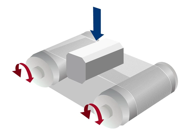
Rough Grinding: This initial phase removes the majority of the material. It is performed under controlled conditions to quickly reduce thickness without inducing too much stress or sub-surface damage.
-
Fine Grinding: Following rough grinding, fine grinding uses finer abrasives to achieve a smoother surface and tighter thickness tolerances. This step is crucial for ensuring the functional quality of the wafers.
-
Surface Uniformity: Face grinding helps to create a uniform surface free from irregularities and defects, which is essential for multicrystalline wafers. Uniform surfaces ensure consistent electrical properties across the wafer, which is crucial for the efficiency of solar cells and the reliability of semiconductor devices.
-
Thickness Accuracy: Precise control of wafer thickness is vital for subsequent processing steps, such as doping and metallization in solar cell manufacturing. Thickness uniformity across a wafer ensures even reaction rates and depths during these processes.
-
Reduced Subsurface Damage: Properly executed face grinding minimizes subsurface damage, which can otherwise lead to weakened wafers and increased breakage rates during handling and further processing.
-
Material Hardness Variation: The varying hardness and abrasiveness of the different crystal grains in multicrystalline silicon can lead to non-uniform material removal rates during grinding, posing challenges in achieving surface uniformity.
-
Stress Management: The grinding process introduces mechanical stresses that can exacerbate the formation of microcracks, particularly along grain boundaries. Managing these stresses through careful control of grinding parameters is essential.
-
Heat Dissipation: Like other abrasive processes, face grinding generates significant heat. Inadequate heat management can lead to thermal damage, affecting the electrical properties and mechanical strength of the wafers.
-
Thickness Consistency: Variations in wafer thickness can lead to problems in subsequent processing steps such as lithography and etching, where uniformity is crucial for patterning and layering accuracy.
-
Surface Flatness: The flatness of wafers affects the ability to uniformly deposit thin films and other materials on their surfaces. Any irregularities can lead to uneven layer thicknesses, which can impede the electrical performance of the finished semiconductor devices.
-
Structural Integrity: Maintaining the structural integrity of wafers during cutting is essential to prevent defects such as microcracks or warping, which could lead to failures during device assembly or operation.
-
Material Quality: The inherent qualities of the silicon material, such as crystal orientation and purity, can affect how it behaves during the cutting process. Inconsistencies in the material can lead to variations in cutting performance and wafer quality.
-
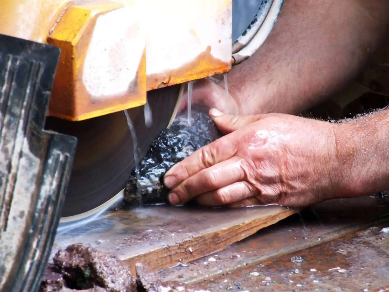
Tool Wear: The precision tools used in wafering undergo wear and tear, which can affect their performance. Regular monitoring and replacement of these tools are necessary to maintain the quality of the cuts.
-
Process Control: The need for precise control over cutting speed, wire tension, and coolant flow is critical. Any deviations can cause fluctuations in wafer thickness and flatness, leading to batch inconsistencies.

Leon Meyer is a veteran manufacturing engineer and technical consultant with over 50 years of experience in the development, implementation, and troubleshooting of industrial diamond tooling systems. Having spent his career at the intersection of tool design, precision manufacturing, and production engineering, Mr. Meyer is widely regarded as one of the most experienced voices in the application of ultra-thin diamond blades, sintered core drills, and CBN grinding wheels across heavy industry, advanced materials, and research sectors.
Known for his pragmatic, no-nonsense approach, Leon has advised manufacturers across the United States, Europe, and East Asia—helping streamline cutting processes, extend tool life, and solve complex issues related to material breakage, chipping, and tolerance drift. His expertise has directly contributed to improved production efficiency in industries ranging from aerospace alloys and technical ceramics to optics, composites, and high-nickel superalloys.
As an author, Mr. Meyer brings a lifetime of field knowledge to his writing, with a focus on real-world problem solving, cost-performance optimization, and tool reliability under demanding conditions.

Guide to Diamond Wire Sawing: Technologies, Wire Types, and Machine Designs
Selecting the Right Diamond Band Saw blade for your Application
Diamond Band Saw Blades Usage Recommendations & Best Practices

Diamond Wire vs band saw blades and circular blades
The Comprehensive Guide to the Processes of Silicon Wafers Production
Manufacturing Processes for Silicon Semiconductors From Ingot to Integrated Circuit
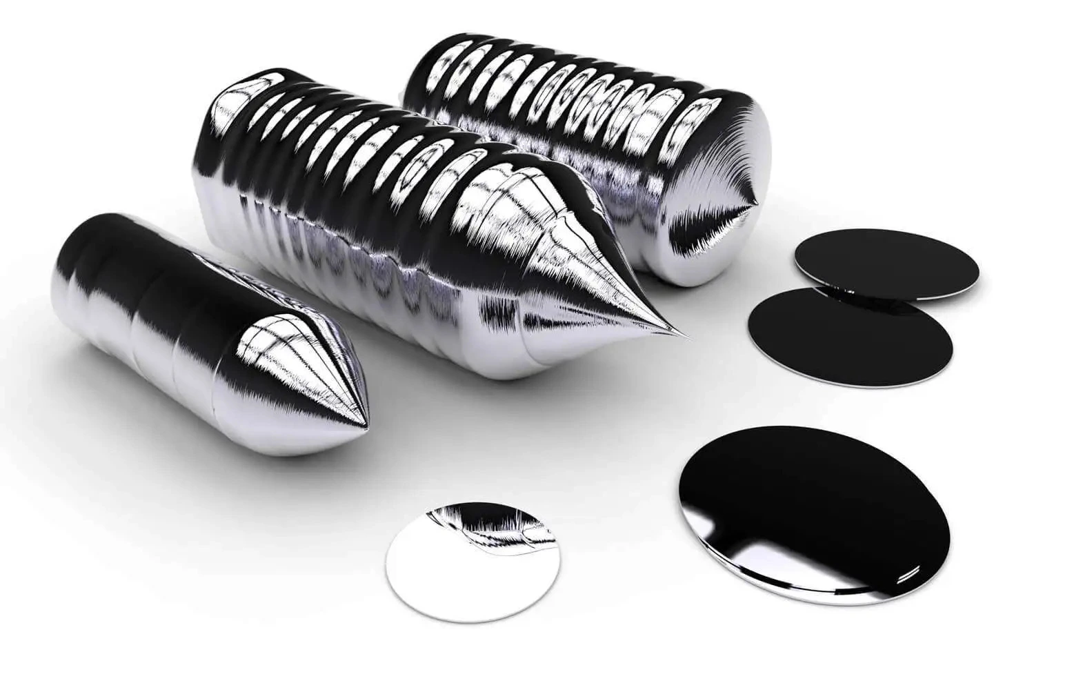
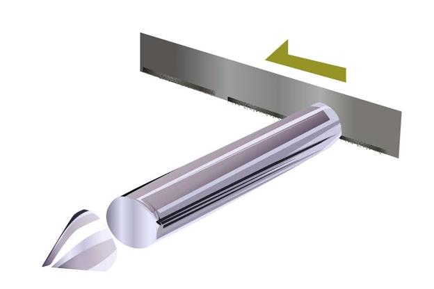
1. Ingot Production The journey begins with the creation of silicon ingots, which are pure silicon cylinders produced through methods like the Czochralski process. Once formed, these ingots undergo a cropping procedure to remove any excess and to prepare them for slicing. This step ensures that only the highest quality silicon is used, which is crucial for the performance of the final semiconductor devices.

Evaluating & Comparing Diamond Blades
Proper testing procedures and methodologies must be set up and used to obtain accurate as well as repeatable testing results. This article will discuss several simple procedures which have been used under actual field conditions, verifying their feasibility for testing diamond cut off wheels.

How to Improve & Optimize Your Diamond Sawing Operation

Troubleshooting Diamond Sawing Problems

Silicon Fabrication Guide

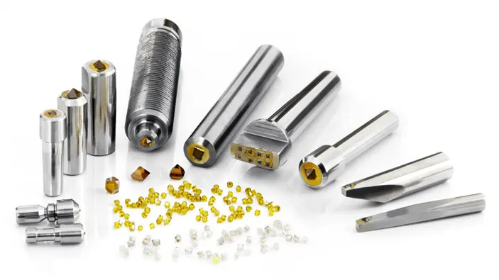
Why use diamond
Diamond is the hardest material known to man kind. When used on diamond/tools, diamond grinds away material on micro (nano) level. Due to its hardness Diamond will work all types of materials from hardness of 40 on Rockwell scale and up. Diamond will machine hardest material, including those materials that other conventional types of abrasives, carbide and high speed steel will not.

How to Selecting Right Diamond Tools for your application
Leon Meyer is a veteran manufacturing engineer and technical consultant with over 50 years of experience in the development, implementation, and troubleshooting of industrial diamond tooling systems. Having spent his career at the intersection of tool design, precision manufacturing, and production engineering, Mr. Meyer is widely regarded as one of the most experienced voices in the application of ultra-thin diamond blades, sintered core drills, and CBN grinding wheels across heavy industry, advanced materials, and research sectors.
Known for his pragmatic, no-nonsense approach, Leon has advised manufacturers across the United States, Europe, and East Asia—helping streamline cutting processes, extend tool life, and solve complex issues related to material breakage, chipping, and tolerance drift. His expertise has directly contributed to improved production efficiency in industries ranging from aerospace alloys and technical ceramics to optics, composites, and high-nickel superalloys.
As an author, Mr. Meyer brings a lifetime of field knowledge to his writing, with a focus on real-world problem solving, cost-performance optimization, and tool reliability under demanding conditions.